
Method for manufacturing solder mask layer on PCB

A solder mask and solder mask technology, applied in transfer printing method, printed circuit manufacturing, coating of non-metallic protective layer, etc., can solve the problems of solder mask ink pollution, excessive development, insufficient development, etc.

Active Publication Date: 2015-12-30
JIANGMEN SUNTAK CIRCUIT TECH
View PDF4 Cites 7 Cited by
  • Summary
  • Abstract
  • Description
  • Claims
  • Application Information

AI Technical Summary

Problems solved by technology

[0003] The present invention is aimed at the prior art when making a solder resist layer on a PCB with a high aspect ratio, a through hole with a window at one end of the pad and an oil-covered solder pad at the other end, and a solder resist bridge with a small width. Excessive or insufficient development will lead to swelling and whitening of the solder mask bridge or pollution of the nickel-coated gold surface by solder mask ink. A method for making a solder mask layer on a PCB is provided. The internal solder resist ink is cleaned and can avoid swelling and whitening of the solder resist bridge

Method used


Image

  • Method for manufacturing solder mask layer on PCB

Examples


Embodiment

[0014] This embodiment provides a method for manufacturing a PCB, especially a method for manufacturing a solder resist layer on a PCB.

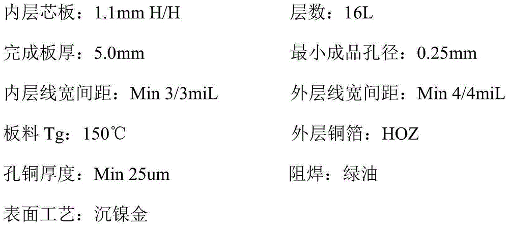
[0015] The specifications of the prepared PCB are as follows:

[0016]

[0017] A via hole with an aperture of 0.25 mm is made on the PCB, and the aspect ratio of the via hole is 12. The pad at one end of the via hole needs to be covered with a solder mask, and the position of the pad is called the oil level; The pad at one end does not need to be covered by a solder mask, and this pad position is called an exposed position.

[0018] Specific steps are as follows:

[0019] (1) Production board with outer circuit

[0020] According to the existing technology, the substrate is made into a production board with an outer circuit by successively cutting the material → negative film process to make the inner layer circuit → pressing → drilling → sinking copper → full board electroplating → positive film process to make the outer layer circuit...


PUM

PropertyMeasurementUnit
Apertureaaaaaaaaaa
Widthaaaaaaaaaa

Abstract

The invention relates to the technical field of circuit board production, in particular to a method for manufacturing a solder mask layer on a PCB. According to the method, the solder mask layer is reinforced through secondary exposure, meanwhile a first shading area and a second shading area are arranged on a secondary film to prevent solder mask ink in a via hole from solidifying, a red adhesive tape is adhered to the position of a solder mask bridge and then secondary development is performed, the solder mask ink left in the via hole can be completely removed, and it can be ensured that the solder mask bridge does not swell and is not whity due to secondary development. The area of the first shading area and the area of the second shading area are set to be greater than those of the corresponding exposed positions and that of the orifice at the coating oil level position, and the problem that the solder mask ink left in the via hole solidifies during secondary development and is difficult to remove can be effectively prevented. By means of the method manufacturing the solder mask layer, the problem that the solder mask ink pollutes the nickel-gold immersion surface during nickel-gold immersion surface treatment can be prevented.

Description

technical field [0001] The invention relates to the technical field of circuit board production, in particular to a method for manufacturing a solder resist layer on a PCB. Background technique [0002] With the diversification and precision development of electronic products, PCB is also developing in the direction of diversification and precision. Some electronic products require PCBs to have via holes with a high aspect ratio, the pad at one end of the via hole is covered with oil (solder mask coverage), the pad at the other end of the via hole is windowed (no solder mask coverage required), and The solder resist bridge with a small width, and the surface treatment of the PCB is immersion nickel gold surface treatment (for example, the aspect ratio of the via hole is 12, the aperture is 0.25mm, and the width of the solder resist bridge is 0.08mm). When making a PCB that meets these three conditions at the same time, development becomes a problem, and it is very easy to h...

Claims


Application Information

Patent Timeline
IPC IPC(8): H05K3/28
CPCH05K3/282H05K2201/099H05K2203/0531
Inventor 汪广明黄力戴勇陈广龙
Owner JIANGMEN SUNTAK CIRCUIT TECH
Learn More