Regenerated ink box chip, regenerated ink box and production process for regenerated ink box

An ink cartridge chip and production process technology, applied in the fields of regenerated ink cartridge chips, regenerated ink cartridges and their production processes, can solve problems affecting the recycling of ink cartridges, short circuits, etc., so as to reduce the risk of virtual welding, improve electrical connection strength, and avoid welding problems. Effect

Inactive Publication Date: 2016-01-06
HANGZHOU CHIPJET TECH
View PDF8 Cites 11 Cited by
  • Summary
  • Abstract
  • Description
  • Claims
  • Application Information

AI Technical Summary

Problems solved by technology

For the repair chip produced by the SMT process, in order to realize the electrical connection between the repair chip and the original chip, the repair chip and the original chip need to be re-soldered. Affects the recycling of ink cartridges

Method used


Image

  • Regenerated ink box chip, regenerated ink box and production process for regenerated ink box
  • Regenerated ink box chip, regenerated ink box and production process for regenerated ink box
  • Regenerated ink box chip, regenerated ink box and production process for regenerated ink box

Examples


Embodiment 1

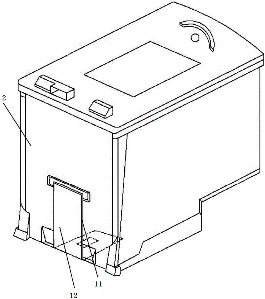
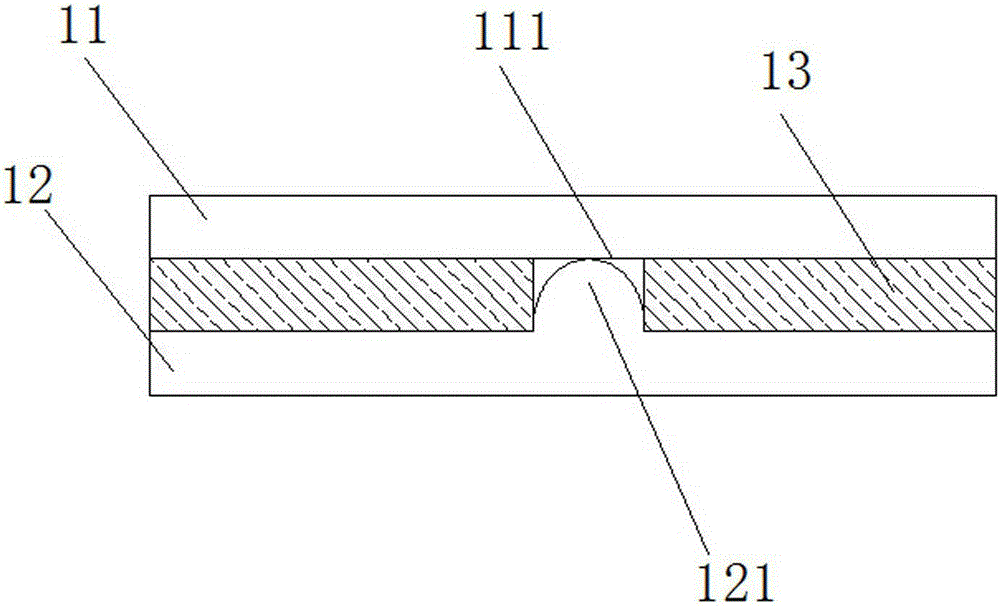
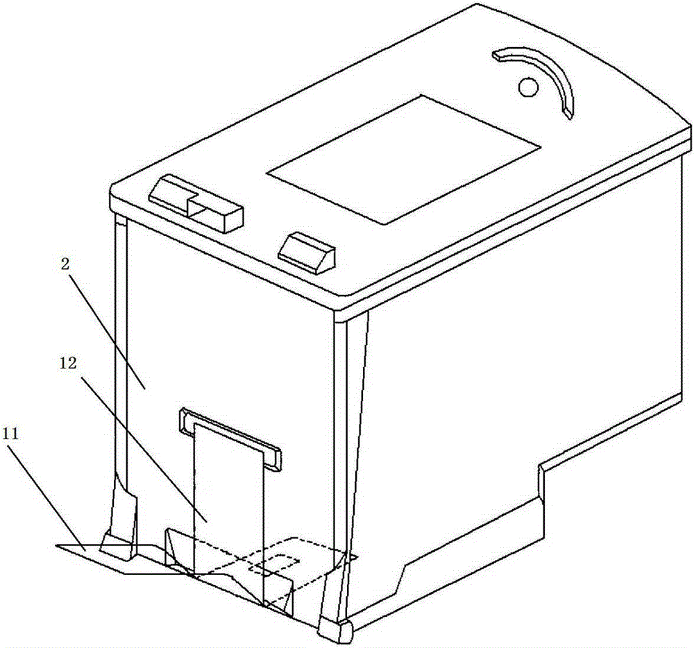
[0049] A regenerated ink cartridge includes a regenerated ink cartridge chip and a container for containing ink. Among them, the structure of the regenerated ink cartridge chip is as follows: figure 2 , including an original chip 11, a repair chip 12, an adhesive layer 13 that is arranged between the original chip 11 and the repair chip 12 and connects the original chip 11 and the repair chip 12; the tin point 121 of the repair chip 12 passes through the adhesive layer 13 and the original Contacts 111 of the chip 11 are contacted. The regenerated ink cartridge chip is installed on the container 2 of the ink cartridge, and the repair chip 12 of the regenerated ink cartridge chip is arranged on the outside of the original chip 11 (such as figure 1 ), so that the original chip 11 is connected to the repair chip 12 and the outer surface of the container 2 . In order to ensure good contact between the repaired chip 12 and the original chip 11 , the thickness of the tin dots 121 ...

Embodiment 2

[0071] Repair chip 12 also can be arranged on former chip 11 inner side (as image 3 ), so that the repair chip 12 is connected to the original chip 11 and the outer surface of the container 2 . In order to prevent other contacts of the original chip 11 from accidentally connecting, improve the safety of the circuit, and prevent interference; ensure that even if the adhesive layer 13 fails, the original chip 11 and the repaired chip 12 are misplaced, and it is not easy to cause a short circuit to cause the chip to break. The phenomenon of burning out. An insulating film 14 can be arranged on the back side of the original chip 11, and the tin point 121 of the repair chip 12 passes through the adhesive layer 13 and the insulating film 14 to contact with the contact 111 of the original chip 11 (such as Figure 4 ). In order to ensure good contact between the repaired chip 12 and the original chip 11 , the thickness of the tin point 121 needs to be the sum of the thicknesses of ...


PUM

PropertyMeasurementUnit
melting pointaaaaaaaaaa

Abstract

The invention relates to the technical field of ink-jet printing imaging, in particular to a regenerated ink box chip, a regenerated ink box and a production process for the regenerated ink box. The regenerated ink box chip comprises an original chip, a restoration chip and a bonding layer which is arranged between the original chip and the restoration chip and connects the original chip with the restoration chip. A tin point of the restoration chip penetrates through the bonding layer to make contact with a contact of the original chip. The restoration chip and the original chip are connected through the bonding layer, so that the relative positions of the restoration chip and the original chip are kept fixed, and good electrical contact between the welding point of the restoration chip and the contact of the original chip is guaranteed.

Description

technical field [0001] The invention relates to the technical field of inkjet printing and imaging, in particular to a regenerated ink cartridge chip, a regenerated ink cartridge and a production process thereof. Background technique [0002] During the printing work, data communication is maintained between the printer and the ink cartridge at any time, and the printer will store the actual ink consumption information in the ink cartridge, until the ink in the ink cartridge is used up, this information will be stored in the ink cartridge, and cannot be changed. When such discarded ink cartridges are loaded into the printer again, the printer will judge the internal data of the ink cartridges (model, origin, date of manufacture, etc.), and read the ink consumption information stored in the ink cartridges to judge the ink volume of the ink cartridges. Since the ink consumption information stored in the ink cartridge cannot be changed, even if the ink cartridge is refilled, t...

Claims


Application Information

Patent Timeline
Patent Type & Authority Applications(China)
IPC IPC(8): B41J2/175B32B7/10B32B3/30
Inventor 傅远贵
Owner HANGZHOU CHIPJET TECH
Why Eureka
Try Eureka