Double-sided display substrate and preparation method and display device thereof

一种双面显示、基板的技术,应用在半导体/固态器件制造、半导体器件、电气元件等方向,能够解决影响OLED双面显示屏良率与显示质量、延长OLED双面显示屏生产周期、不利OLED双面显示屏快速推广等问题,达到快速制备与推广、提升良率和显示质量、降低制备成本与能耗成本的效果

Active Publication Date: 2016-01-06
BOE TECH GRP CO LTD +1
View PDF4 Cites 17 Cited by
  • Summary
  • Abstract
  • Description
  • Claims
  • Application Information

AI Technical Summary

Problems solved by technology

The preparation process of this method is complicated, and each layer structure in the OLED screen and the thin-film transistor driving circuit need to be prepared in duplicate, which is not only not conducive to reducing the preparation cost and energy consumption cost of the double-sided OLED display screen, but also has excessive thickness and volume. Large, heavy and other shortcomings; at the same time, it will also affect the yield and display quality of OLED double-sided displays
The above defects not only prolong the production cycle of OLED double-sided display, but also are not conducive to the rapid promotion of OLED double-sided display in the market

Method used


Image

  • Double-sided display substrate and preparation method and display device thereof
  • Double-sided display substrate and preparation method and display device thereof
  • Double-sided display substrate and preparation method and display device thereof

Examples


Embodiment 1

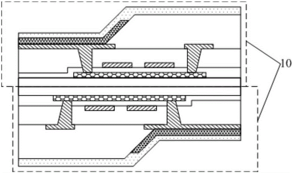
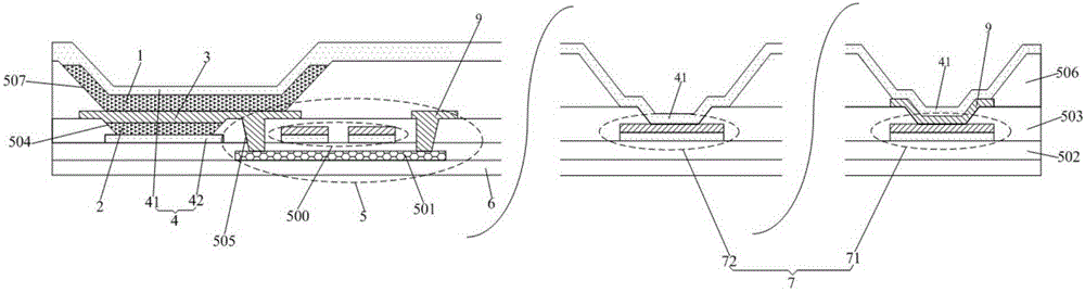
[0051] This embodiment provides a double-sided display substrate, including several sub-pixel units arranged in the pixel area, such as figure 2 As shown, the sub-pixel unit includes a front light emitting layer 1 for front display, a back light emitting layer 2 for back display, a pixel electrode layer 3, a common electrode layer 4 and a driving transistor 5, and the front light emitting layer 1 and the back light emitting layer 2 They are respectively sandwiched between the corresponding pixel electrode layer 3 and the common electrode layer 4, and the driving transistor 5 is used to control the front light emitting layer 1 and the back light emitting layer 2 to emit light, and the common electrode layer 4 corresponding to the back light emitting layer 2 is connected to the drive The gate electrode layer 500 of the transistor 5 is provided in the same layer.

[0052] In this embodiment, the sub-pixel unit includes a driving transistor 5, and the driving transistor 5 is used...

Embodiment 2

[0078] This embodiment provides a double-sided display substrate, which is different from Embodiment 1, as Figure 16 As shown, the sub-pixel unit includes a first drive transistor 51 for controlling the light emission of the front light-emitting layer 1 and a second drive transistor 52 for controlling the light emission of the back light-emitting layer 2. The first drive transistor 51 and the second drive transistor 52 share the same The gate electrode layer 500; the pixel electrode layer 3 includes a first pixel electrode layer 31 corresponding to the front light emitting layer 1 and a second pixel electrode layer 32 corresponding to the back light emitting layer 2, and the front light emitting layer 1 and the back light emitting layer 2 share the same common electrode layer 4. The common electrode layer 4 and the gate electrode layer 500 are arranged on the same layer.

[0079] Such an arrangement enables the first drive transistor 51 and the second drive transistor 52 to c...

Embodiment 3

[0085] This embodiment provides a double-sided display substrate, which is different from Embodiment 1-2, as Figure 17As shown, the sub-pixel unit includes a first drive transistor 51 for controlling the light emission of the front light-emitting layer 1 and a second drive transistor 52 for controlling the light emission of the back light-emitting layer 2. The first drive transistor 51 and the second drive transistor 52 share the same Gate electrode layer 500; the pixel electrode layer 3 includes the first pixel electrode layer 31 corresponding to the front light emitting layer 1 and the second pixel electrode layer 32 corresponding to the back light emitting layer 2, and the common electrode layer 4 includes the first common electrode layer corresponding to the front light emitting layer 1. The electrode layer 41 and the second common electrode layer 42 corresponding to the light-emitting layer 2 on the opposite side, the first common electrode layer 41 , the second common el...


PUM


Abstract

The invention provides a double-sided display substrate and a preparation method and a display device thereof. The double-sided display substrate comprises a plurality of sub-pixel units, wherein each sub-pixel unit comprises a front luminescent layer, a reverse luminescent layer, a pixel electrode layer, a common electrode layer and a drive transistor; each front luminescent layer is used for carrying out front displaying; each reverse luminescent layer is used for carrying out reverse displaying; each front luminescent layer and each reverse luminescent layer are respectively clamped between the corresponding pixel electrode layer and common electrode layer; each drive transistor is used for controlling the corresponding front luminescent layer and reverse luminescent layer to shine; and the common electrode layers corresponding to the front luminescent layers and / or the reverse luminescent layers, and gate electrode layers of the drive transistors are arranged on the same layer. According to the double-sided display substrate, the thickness and the volumeof the double-sided display substrate can be effectively reduced; the preparation cost and the energy consumption cost of the double-sided display substrate are reduced; the design difficulty is lowered; the production cycle of the display substrate is shortened; and the yield and the display quality of the display substrate are improved, so that rapid preparation and popularization of the double-sided display substrate are achieved.

Description

technical field [0001] The present invention relates to the field of display technology, in particular to a double-sided display substrate, a preparation method thereof, and a display device. Background technique [0002] More and more attention has been paid to display products that use thin-film transistors as control elements and organic electroluminescent devices (OLEDs) as light-emitting media because of their advantages such as high definition, wide viewing angles, and easy realization of flexible and flexible displays. [0003] With the application of OLED display products, OLED display screens with double-sided display effects are required in more and more occasions. At present, the double-sided display OLED display mainly adopts the method of laminating two single-sided OLED screens 10 to realize the double-sided display effect, such as figure 1 shown. The preparation process of this method is complicated, and each film layer structure in the OLED screen and the t...

Claims


Application Information

Patent Timeline
Patent Type & Authority Applications(China)
IPC IPC(8): H01L27/12H01L21/77
CPCH01L27/1214H01L27/1259H01L27/1218H01L27/1222H01L27/1266H10K59/121H10K59/176H10K59/1201
Inventor 李坤
Owner BOE TECH GRP CO LTD
Why Eureka
Try Eureka