Surface-enhanced Raman scattering substrate with pin holes in its surface and preparation method

A surface-enhanced Raman and pinhole technology, which is applied in Raman scattering, material excitation analysis, etc., can solve problems such as weak adsorption capacity, poor chemical stability of metal nanostructures, and limit the development of surface-enhanced Raman technology. Application range, good surface to enhance Raman activity, and the effect of improving chemical stability

Active Publication Date: 2016-01-13
广西三环高科拉曼芯片技术有限公司
View PDF4 Cites 4 Cited by
  • Summary
  • Abstract
  • Description
  • Claims
  • Application Information

AI Technical Summary

Problems solved by technology

This method requires the use of precious metals such as gold and silver to prepare surface-enhanced Raman effect substrates with high sensitivity. At the same time, due to the poor ch

Method used


Image

  • Surface-enhanced Raman scattering substrate with pin holes in its surface and preparation method
  • Surface-enhanced Raman scattering substrate with pin holes in its surface and preparation method
  • Surface-enhanced Raman scattering substrate with pin holes in its surface and preparation method

Examples


Embodiment 1

[0019] 1. Clean the silicon substrate or glass substrate sequentially with acetone, alcohol and deionized water and dry them;

[0020] 2. Fix the pretreated substrate on the sample stage of the electron beam evaporation coating machine;

[0021] 3. At room temperature, using metallic silver as the target material, pump the chamber of the electron beam evaporation coating machine to a vacuum degree of 3×10 -5 Pa;

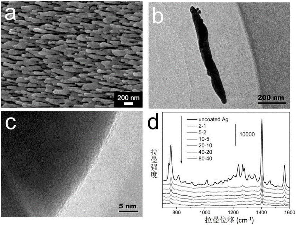
[0022] 4. Adjust the incident angle of the electron beam to 85°, and make the sample stage static, and grow a silver nanorod array thin film with a nanorod length of 700nm obliquely on the substrate of the sample stage;

[0023] 5. By the low-temperature atomic layer deposition method, heat the chamber to 70°C, control the flow rate of trimethylaluminum and water to 20 sccm, and control the pinhole ratio of the aluminum oxide film by adjusting the time of trimethylaluminum and water, The penetration time of trimethylaluminum is 2ms, 5ms, 10ms, 20ms, 40ms, 80ms resp...

Embodiment 2

[0028] 1. Clean the silicon substrate or glass substrate sequentially with acetone, alcohol and deionized water and dry them;

[0029] 2. Fix the pretreated substrate on the sample stage of the electron beam evaporation coating machine;

[0030] 3. At room temperature, using metallic silver as the target material, pump the chamber of the electron beam evaporation coating machine to a vacuum degree of 5×10 -5 Pa;

[0031] 4. Adjust the incident angle of the electron beam to 86°, and make the sample stage rotate at a rate of 6rpm, and grow a silver nanorod array film with a nanorod length of 600nm obliquely on the substrate of the sample stage;

[0032] 5. Through the low-temperature atomic layer deposition method, heat the chamber to 60°C, control the flow rate of trimethylaluminum and water to 20sccm, and the feeding time is 10ms and 5ms respectively, and uniformly deposit a layer on the surface of the silver nanorod array film with Alumina film with pinholes, to obtain a silv...

Embodiment 3

[0037] 1. Clean the silicon wafer substrate or glass substrate sequentially with acetone, alcohol, and deionized water, and then dry it;

[0038] 2. Fix the pretreated substrate on the sample stage of the electron beam evaporation coating machine;

[0039] 3. At room temperature, use metallic silver as the target material, pump the chamber of the electron beam evaporation coating machine to 8×10 -5 Pa high vacuum;

[0040] 4. Adjust the incident angle of the electron beam to 88°, and make the sample stage rotate at a rate of 10rpm, and grow a silver nanocylindrical straight rod array film with a nanorod length of 400nm on the substrate of the sample stage;

[0041] 5. Through the low-temperature atomic layer deposition method, heat the chamber to 50°C, control the flow rate of trimethylaluminum and water to 20sccm, and the feeding time is 80ms and 40ms respectively, and uniformly deposit a layer on the surface of the silver nanocylindrical straight rod array film Alumina fil...


PUM

PropertyMeasurementUnit
Lengthaaaaaaaaaa
Thicknessaaaaaaaaaa
Lengthaaaaaaaaaa

Abstract

The invention especially relates to a surface-enhanced Raman scattering substrate with pin holes in its surface and a preparation method, belonging to the technical field of detection of trace substances. According to the invention, a silver nanorod array film is prepared by using an inclined growth process; and then a layer of an alumina film with pin holes is uniformly deposited on the surface of the silver nanorod array film by using low-temperature atomic layer deposition technology, and an obtained sliver-alumina composite nanostructure with pin holes in its surface is used as the surface-enhanced Raman scattering substrate. The method can adjust the parameters of the low-temperature atomic layer deposition technology to control the proportion of the pin holes in the alumina film; an ultrathin oxide layer of the alumina film ensures good surface-enhanced Raman scattering activity of the substrate; and interior silver nanorods are isolated from the outside, so chemical stability of the substrate is greatly improved. Moreover, the alumina film and silver surface layers in the pin holes can both adsorb specific detection molecules; and the substrate is applicable to detection of a plurality of chemical substances, expands the application scope of surface-enhanced Raman scattering and has wide application prospects.

Description

technical field [0001] The invention belongs to the technical field of trace substance detection, and in particular relates to a surface-enhanced Raman effect substrate with pinholes on the surface and a preparation method thereof. Background technique [0002] The surface-enhanced Raman effect is used in the trace detection of chemical and biological molecules, and has the advantages of non-destructive analysis, high sensitivity, short detection time, low cost, and strong applicability. This method requires the use of precious metals such as gold and silver to prepare surface-enhanced Raman effect substrates with high sensitivity. At the same time, due to the poor chemical stability of metal nanostructures and the weak adsorption capacity for some detection molecules, the surface-enhanced Raman effect is greatly limited. technology development. [0003] In the present invention, a layer of ultra-thin aluminum oxide film with pinholes is deposited on the surface of the silv...

Claims


Application Information

Patent Timeline
IPC IPC(8): G01N21/65
Inventor 张政军马菱薇
Owner 广西三环高科拉曼芯片技术有限公司
Why Eureka
Try Eureka