Flip-chip bonding welded spot defect detection method
A detection method and point defect technology, which is applied in the field of flip-chip packaging, can solve the problems of detection and research of small defects in small structures
- Summary
- Abstract
- Description
- Claims
- Application Information
AI Technical Summary
Problems solved by technology
Method used
Image

Examples
Embodiment
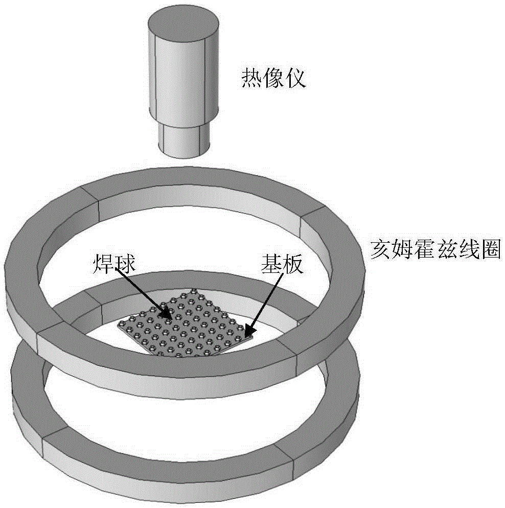
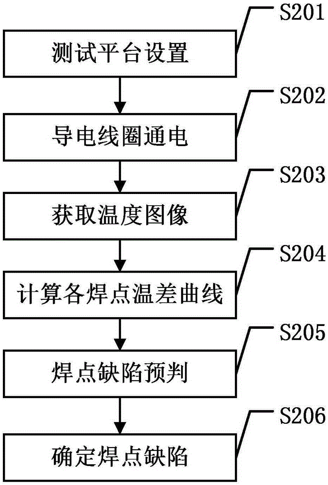
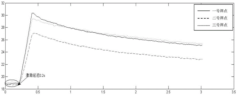
[0049] In order to illustrate the effectiveness of the present invention, experiments were conducted using specific flip-chip solder joints. For the sake of illustration, only three solder joints with a diameter of 1 mm were collected in this test, which are hollow solder joints, crack solder joints, and qualified solder joints, which are recorded as No. 1 solder joint, No. 2 solder joint and No. 3 solder joint. point, take the threshold Δ 1 = 1.0, Δ 2 =-2.0. The excitation current of the conductive coil is set to 220A, the frequency is 250kHz, the coil is placed horizontally, the lifting distance is 0mm, and the heating time and cooling time are 0.2s and 2.8s, respectively. Obtain temperature profiles for the three solder joints. image 3 is the temperature profile of the three solder joints. Such as image 3 It can be seen that the trends of the temperature curves of the three solder joints are consistent. Directly use the temperature curve of the qualified solder join...
PUM
 Abstract
Description
Claims
Application Information
 - R&D
- Intellectual Property
- Life Sciences
- Materials
- Tech Scout
- Unparalleled Data Quality
- Higher Quality Content
- 60% Fewer Hallucinations
Browse by: Latest US Patents, China's latest patents, Technical Efficacy Thesaurus, Application Domain, Technology Topic, Popular Technical Reports.
© 2025 PatSnap. All rights reserved.Legal|Privacy policy|Modern Slavery Act Transparency Statement|Sitemap|About US| Contact US: help@patsnap.com