
AMOLED drive device

A driving device and driving signal technology, applied in static indicators, instruments, etc., can solve the problem of high requirements for drive chip transmission speed and memory access speed, and achieve high requirements for access speed, lower requirements, and lower data volume effect

Active Publication Date: 2016-01-13
SHENZHEN CHINA STAR OPTOELECTRONICS TECH CO LTD
View PDF4 Cites 5 Cited by
  • Summary
  • Abstract
  • Description
  • Claims
  • Application Information

AI Technical Summary

Problems solved by technology

[0006] The purpose of the present invention is to provide a kind of AMOLED driving device that requires lower transmission speed of the driving chip and the access speed of the memory; higher technical issues

Method used


Image

  • AMOLED drive device
  • AMOLED drive device

Examples


Embodiment Construction

[0039] The following descriptions of the various embodiments refer to the accompanying drawings to illustrate specific embodiments in which the present invention can be practiced. The directional terms mentioned in the present invention, such as "up", "down", "front", "back", "left", "right", "inside", "outside", "side", etc., are for reference only The orientation of the attached schema. Therefore, the directional terms used are used to illustrate and understand the present invention, but not to limit the present invention.

[0040] In the figures, structurally similar units are denoted by the same reference numerals.

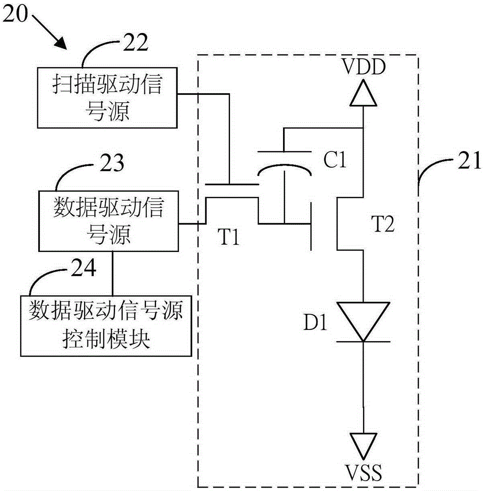
[0041] Please refer to figure 2 , figure 2 It is a structural schematic diagram of a preferred embodiment of the AMOLED driving device of the present invention. The AMOLED driving device 20 of this preferred embodiment includes an AMOLED driving circuit 21 , a scan driving signal source 22 , a data driving signal source 23 and a data driving signal sourc...


PUM


Abstract

The invention provides an AMOLED drive device which comprises an AMOLED drive circuit, a scanning drive signal source, a data driving signal source and a data driving signal source control module. The AMOLED drive circuit comprises a first semiconductor controllable switch, a second semiconductor controllable switch, an energy-storage capacitor and an organic light-emitting diode; the scanning drive signal source is used for generating scanning drive signals; the data driving signal source is used for generating data driving signals; and the data driving signal source control module is used for controlling the working mode of the data driving signal source. The AMOLED drive device carries out division on gray-scale value of each pixel, thereby reducing data volume of each PWM drive signal, and reducing transmission speed for a drive chip and requirement for storage speed of a storage device.

Description

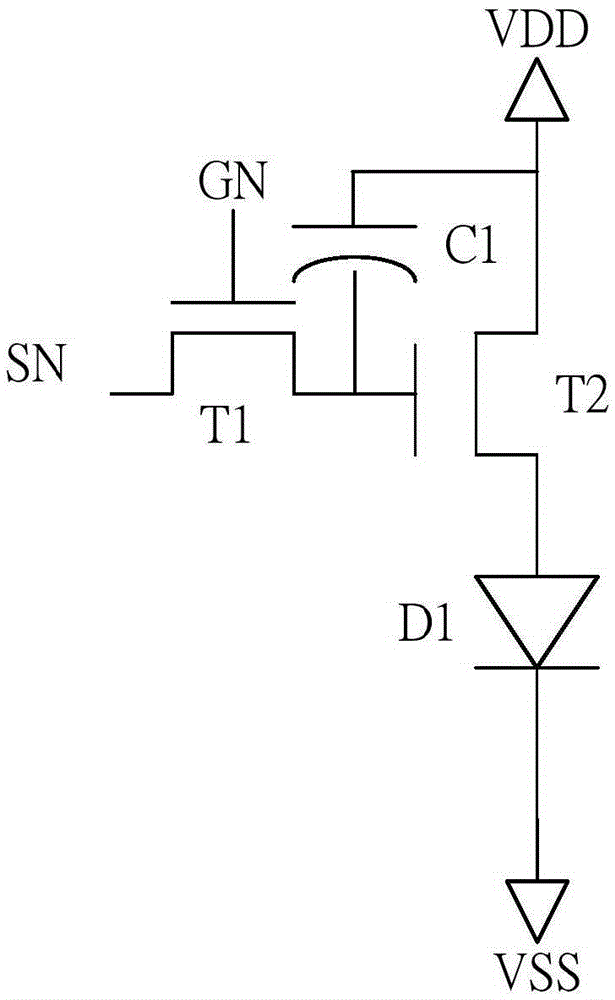
technical field [0001] The invention relates to the field of electronic display, in particular to an AMOLED driving device. Background technique [0002] Due to the advances in process technology and materials of flat-panel displays, organic light-emitting diodes (AMOLED, Active-matrixorganiclight-emittingdiode) will slowly become the mainstream of future displays. [0003] figure 1 Shown is a conventional AMOLED driving circuit, which includes a first semiconductor controllable switch T1, a second semiconductor controllable switch T2, an energy storage capacitor C1 and an organic light emitting diode D1. One end of the second semiconductor controllable switch T2 is connected to the first control voltage VDD, the other end is connected to the anode of the organic light emitting diode D1, the negative electrode of the organic light emitting diode D1 is connected to the second control voltage VSS, the first semiconductor controllable The source of the switch T1 is connected ...

Claims


Application Information

Patent Timeline
Patent Type & Authority Applications(China)
IPC IPC(8): G09G3/3225
CPCG09G3/2018G09G3/3233G09G2320/0271G09G2340/0428G09G3/3266G09G3/3291G09G2300/0408G09G2310/027G09G2310/08
Inventor 温亦谦
Owner SHENZHEN CHINA STAR OPTOELECTRONICS TECH CO LTD
Learn More