Method for holding thin wafer through temporary bonding of porous slide glass

A technology for temporary bonding and thin wafers, which is applied in the manufacture of electrical components, electrical solid devices, semiconductor/solid devices, etc., to achieve the effects of reducing usage, avoiding poor heat dissipation, and easy heat dissipation

Active Publication Date: 2016-01-13
HUATIAN TECH KUNSHAN ELECTRONICS
View PDF8 Cites 8 Cited by
  • Summary
  • Abstract
  • Description
  • Claims
  • Application Information

AI Technical Summary

Problems solved by technology

[0005] In order to solve the above-mentioned technical problems, the present invention proposes a method for temporarily bonding a porous carrier to hold a thin wafer. When temporarily bonding a wafer with a bump structure, the thickness of the bon...

Method used


Image

  • Method for holding thin wafer through temporary bonding of porous slide glass
  • Method for holding thin wafer through temporary bonding of porous slide glass
  • Method for holding thin wafer through temporary bonding of porous slide glass

Examples


Embodiment Construction

[0029] In order to make the present invention more comprehensible, the specific implementation manners of the present invention will be described in detail below in conjunction with the accompanying drawings. For convenience of description, the components in the structures in the drawings of the embodiments are not scaled according to the normal scale, so they do not represent the actual relative sizes of the structures in the embodiments.

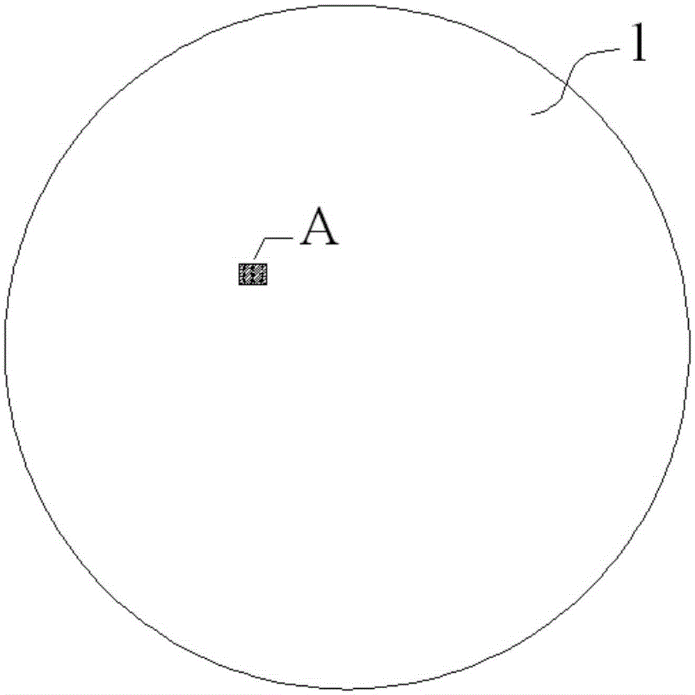
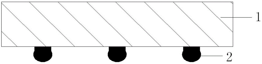
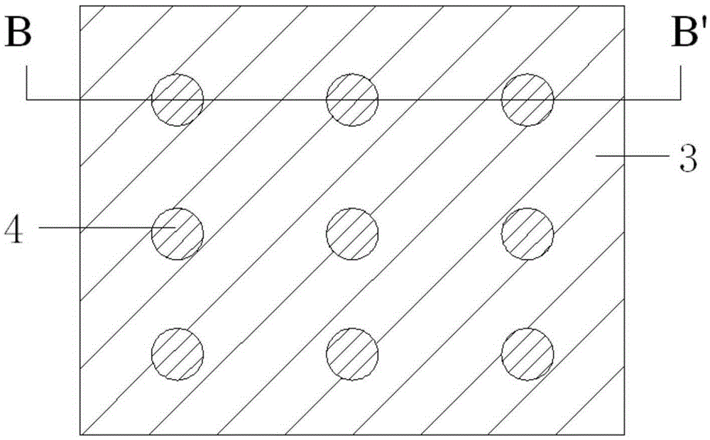
[0030] Such as figure 1 , figure 2 , image 3 , Figure 4 and Figure 5 As shown, a method for temporarily bonding and holding a thin wafer on a porous carrier, through the method of temporarily bonding glue, a wafer 1 with a number of bumps 2 on the front and a wafer 1 with a number of relief slots 4 on the surface The temporary carrier 3 is bonded together, and the higher bumps or all the bumps are inserted into the relief slots on the temporary carrier; after the back process of the wafer is completed, it is immersed in the chemica...


PUM

PropertyMeasurementUnit
Thicknessaaaaaaaaaa
Heightaaaaaaaaaa
Thicknessaaaaaaaaaa

Abstract

The present invention discloses a method for holding a thin wafer through temporary bonding of porous slide glass. The temporary slide glass is provided with abdicating slotted holes with the amount not less than the amount of bumps on the wafer, and the abdicating slotted holes are in response to the bumps on the wafer so as to allow the higher bumps at the front wafer surface or all the bumps to insert into the abdicating slotted holes on the temporary slide glass. The thickness of bonding glue may be effectively reduced, the usage amount of the bonding glue may be decreased, and the heat radiation is easy, therefore process problems caused by poor heat radiation of thick glue in the subsequent process may be avoided. Preferably, the abdicating slotted holes are designed to be a through-hole mode, when the abdicating slotted holes are immersed into a chemical solution for bonding removal, the temporary bonding glue may be dissolved through the through holes on the temporary slide glass after completing the wafer back process, and the bonding removal is completed so as to accelerate the de-bonding efficiency.

Description

technical field [0001] The invention relates to the technical field of semiconductor packaging, in particular to a method for holding a thin wafer. Background technique [0002] Wafer thinning is one of the key process steps to achieve ultra-thin packaging and TSV-based 3D integration technology. barriers and reduce costs. [0003] However, the thickness of the wafer becomes smaller and smaller, and its hardness becomes smaller and smaller, especially when the wafer is thinned to 100 μm or even thinner, the thin wafer will be easily warped, and even a small force will cause the wafer to collapse. rupture. Etching, metal interconnection, etc. on the backside of the thinned wafer can easily cause debris. Temporary bonding and debonding is an effective solution for holding thin wafers. It mainly uses the temporary carrier to provide sufficient mechanical support for the thin wafer. After the wafer back process is completed, the temporary carrier is easily removed from the wa...

Claims


Application Information

Patent Timeline
IPC IPC(8): H01L21/683
CPCH01L21/6835H01L2221/68318H01L2221/68363
Inventor 于大全范俊
Owner HUATIAN TECH KUNSHAN ELECTRONICS
Why Eureka
Try Eureka