
Organic electroluminescent device, its manufacturing method, and display device

An electroluminescent device and luminescent technology, applied in the direction of organic light-emitting devices, organic light-emitting device parameters, organic semiconductor devices, etc., can solve the problems of light-emitting devices such as reduced luminous efficiency and life, and different numbers of electrons and holes. Effect of improving luminous efficiency and life

Active Publication Date: 2018-06-29
BOE TECH GRP CO LTD +1
View PDF16 Cites 0 Cited by
  • Summary
  • Abstract
  • Description
  • Claims
  • Application Information

AI Technical Summary

Problems solved by technology

[0005] The inventors have found that there are at least the following problems in the prior art: since electrons and holes have different injection rates, that is, the electron injection rate is greater than the hole injection rate, the number of electrons and holes injected into the recombination region of the light-emitting layer will be different, As a result, the luminous efficiency and lifetime of organic electroluminescent devices are reduced

Method used


Image

  • Organic electroluminescent device, its manufacturing method, and display device
  • Organic electroluminescent device, its manufacturing method, and display device
  • Organic electroluminescent device, its manufacturing method, and display device

Examples


Embodiment 1

[0065] This embodiment provides an organic electroluminescence device, an anode layer, a cathode layer, and a luminescent layer disposed between the anode layer and the cathode layer; wherein, at least one of the anode layer and the cathode layer is disposed between the luminescent layer There is a carrier speed adjustment layer; the carrier speed adjustment layer is used to adjust the injection rate of carriers.

[0066] When driving the organic electroluminescent device to emit light, because the injection rate of the anode layer injecting holes into the light-emitting layer is different from that of the cathode layer injecting electrons into the light-emitting layer, that is, the hole injection rate is lower than the electron injection rate, which will lead to the injection into the light-emitting layer at the same time. The number of electrons and the number of holes in the layer recombination area are different, so the luminous efficiency and lifespan of the organic electr...

Embodiment 2

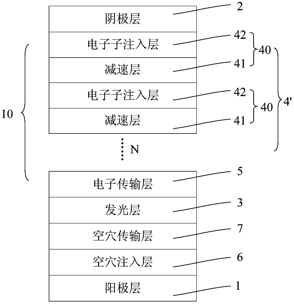
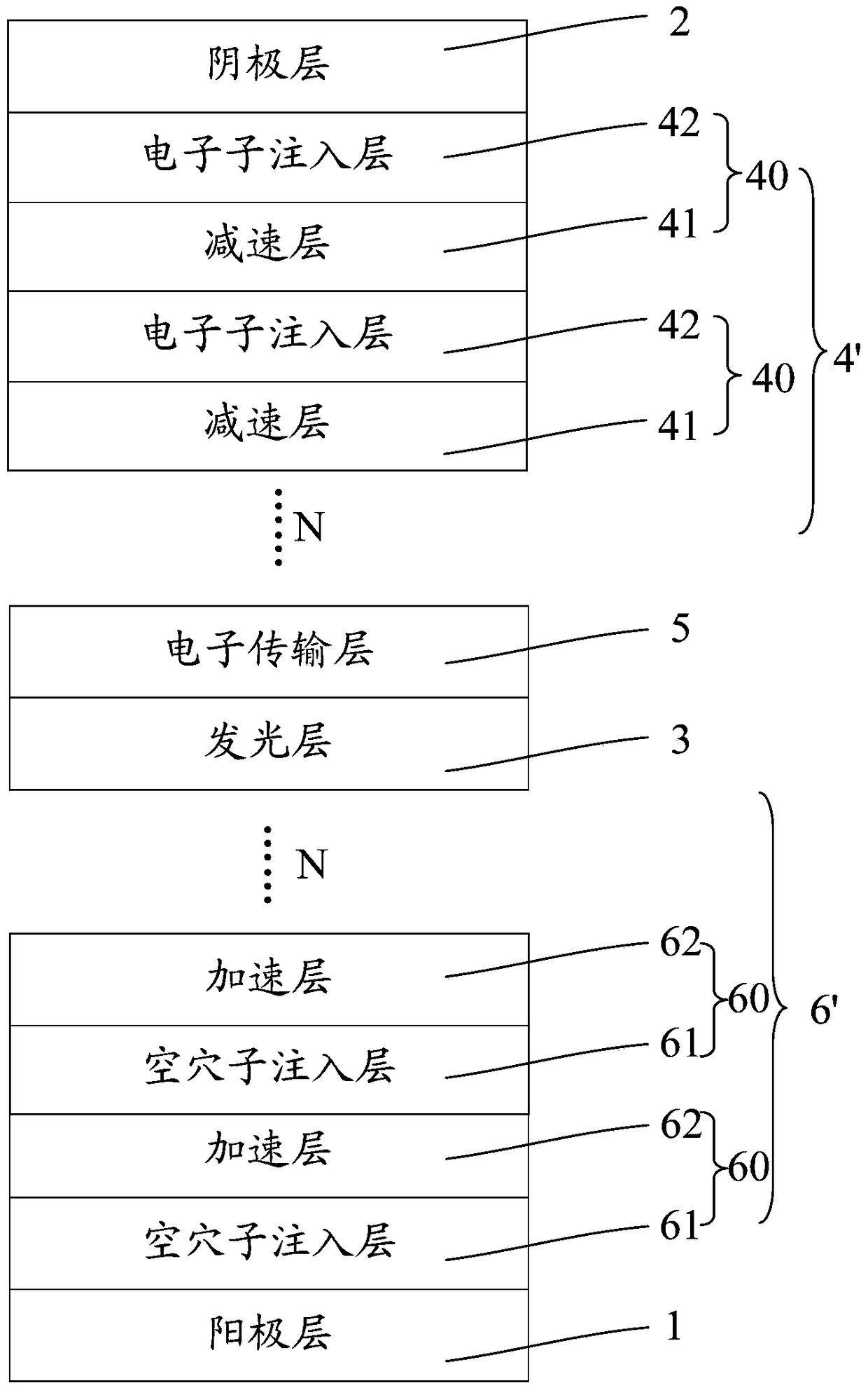
[0068] Such as figure 1 As shown, the present embodiment provides an organic electroluminescent device and a preparation method thereof. The organic electroluminescent device includes an anode layer 1 , a light emitting layer 3 , a carrier velocity adjustment layer 10 , and a cathode layer 2 . Wherein, the carrier speed adjustment layer 10 in this embodiment at least includes an electron speed adjustment layer 4'; the electron speed adjustment layer 4' includes a plurality of electron trap units 40 arranged continuously, and the electron trap units 40 include The electron sub-injection layer 42 and the deceleration layer 41 arranged in sequence in the direction of the cathode layer; wherein the electron sub-injection layer 42 is used to inject electrons into the deceleration layer 41; the deceleration layer 41 is used to slow down the electron injection rate.

[0069] That is to say, when the organic electroluminescent device is applied with an external voltage, the electrons ...

Embodiment 3

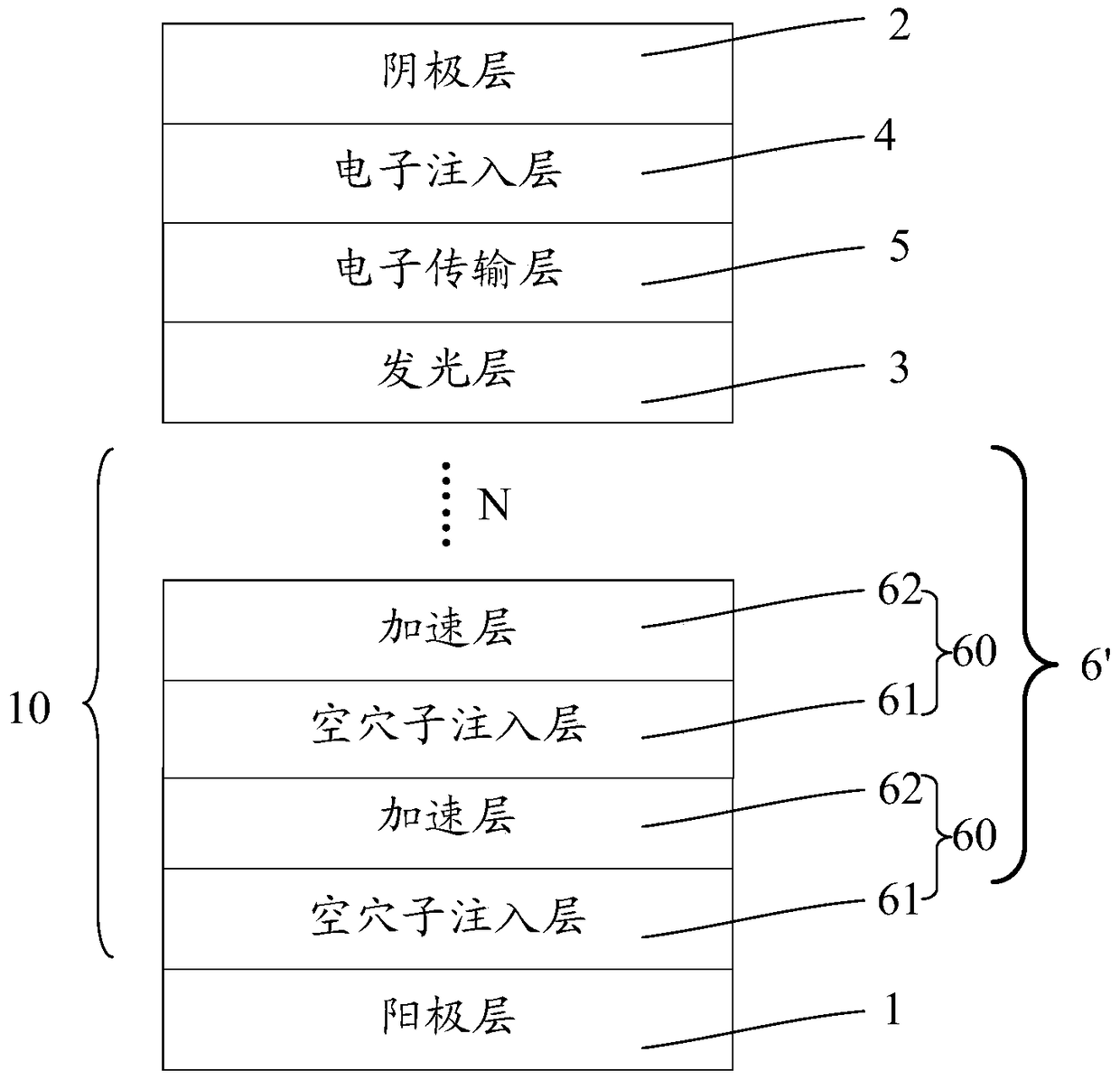
[0095] Such as figure 2 As shown, the present embodiment provides an organic electroluminescent device and a preparation method thereof. The organic electroluminescent device includes a substrate, an anode layer 1, a carrier velocity adjustment layer 10, and a light-emitting layer 3 arranged on the substrate in sequence, and the cathode layer 2 . Wherein, the carrier speed adjustment layer 10 in this embodiment includes a hole speed adjustment layer 6'; the hole speed adjustment layer 6' includes a plurality of hole acceleration units 60 arranged continuously; each hole acceleration unit 60 It includes a hole injection layer 61 and an acceleration layer 62 arranged in sequence along the direction away from the anode layer 1; wherein, the hole injection layer 61 is used to inject holes into the acceleration layer 62; the acceleration layer 62 is used to increase the hole Injection rate.

[0096] In this embodiment, since the carrier velocity adjustment layer 10 is added betw...


PUM


Abstract

The invention provides an organic electroluminescent device, its preparation method and display device, belonging to the field of display technology, which can solve the problem of low luminous efficiency and short service life caused by the different injection rates of electrons and holes in existing organic electroluminescent devices The problem. The organic electroluminescent device of the present invention comprises an anode layer, a cathode layer, and a luminescent layer disposed between the anode layer and the cathode layer, and the organic electroluminescence device further comprises: A carrier velocity adjustment layer between at least one of them and the light-emitting layer; the carrier velocity adjustment layer is used to adjust the injection rate of carriers.

Description

technical field [0001] The invention belongs to the field of display technology, and in particular relates to an organic electroluminescence device, a preparation method thereof, and a display device. Background technique [0002] OLED (Organic Light-Emitting Device: Organic Light-Emitting Device, referred to as OLED) is a light-emitting device that uses organic solid-state semiconductors as light-emitting materials. The wide temperature range and other advantages make it have broad application prospects. [0003] The structure of an existing OLED generally includes an anode layer, a cathode layer, and an organic functional layer arranged between the anode layer and the cathode layer, and the organic functional layer includes a hole injection layer, a hole transport layer, and , light emitting layer, electron transport layer, and electron injection layer. Wherein, the hole injection layer is adjacent to the anode layer, and the electron injection layer is adjacent to the c...

Claims


Application Information

Patent Timeline
Patent Type & Authority Patents(China)
IPC IPC(8): H01L51/50H01L51/56H10K99/00
CPCH10K50/171H10K50/85H10K50/16H10K2101/40H10K50/156H10K2102/351H10K50/15H10K50/17H10K85/1135H10K50/166H10K50/00H10K50/81H10K50/82H10K71/00H10K85/60H10K85/631H10K85/654H10K85/6565H10K85/6572H10K2101/00H10K2102/00
Inventor 吴海东赖韦霖陈凯白娟娟马文昱
Owner BOE TECH GRP CO LTD
Learn More