Liquid crystal display apparatus

A liquid crystal display device and substrate technology, which is applied in nonlinear optics, instruments, optics, etc., can solve the problem of magenta in the chromaticity of the screen, and achieve the effects of reducing hue shift, reducing time constant, and reducing the effect

Active Publication Date: 2016-01-27
TIANMA MICRO ELECTRONICS CO LTD
View PDF7 Cites 5 Cited by
  • Summary
  • Abstract
  • Description
  • Claims
  • Application Information

AI Technical Summary

Problems solved by technology

On the contrary, in the case of a normally white display system, since the brightness of the green pixel is lower than

Method used


Image

  • Liquid crystal display apparatus
  • Liquid crystal display apparatus
  • Liquid crystal display apparatus

Examples


Embodiment approach 1

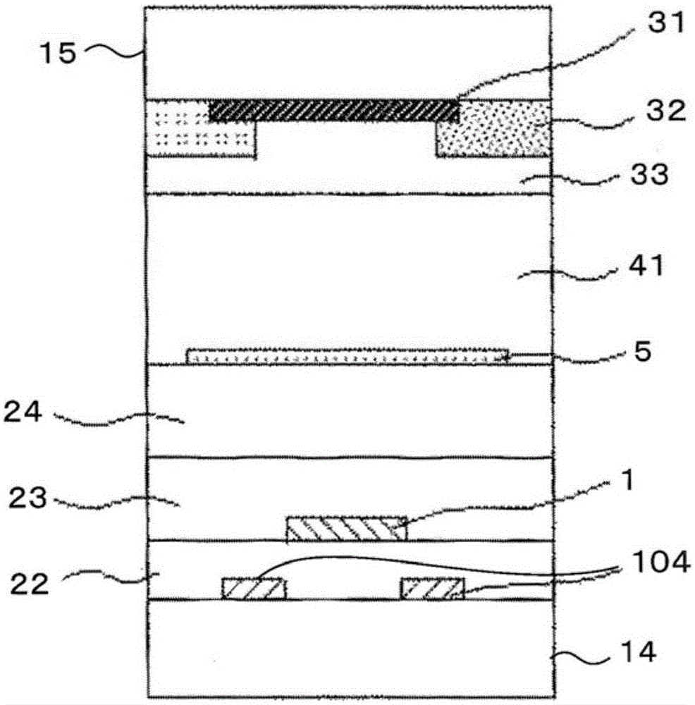
[0074] Hereinafter, the embodiments of the present invention described above will be described in more detail. will refer to Figure 7A to Figure 7C as well as Figure 8A and Figure 8B The structure of the liquid crystal display device according to Embodiment Mode 1 of the present invention will be described. Figure 7A is a top view of this embodiment, Figure 7B and Figure 7C for Figure 7A cutaway view.

[0075] The liquid crystal display device of the present embodiment includes: a transparent substrate (hereinafter referred to as "TFT substrate" (first substrate)) 14, signal wiring 1, scanning wiring 2, pixel electrode 6, counter electrode 7, and Similar elements for driving an electric field of liquid crystals are provided on a transparent substrate 14; a transparent substrate (hereinafter referred to as "color filter substrate" (second substrate)) 15, a black matrix 31, a color filter element 32 and a planarization layer 33 is provided on the transparent substr...

Embodiment approach 2

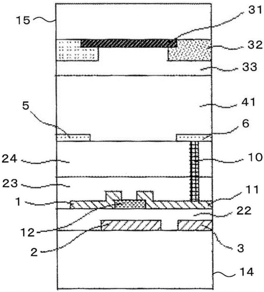
[0096] will refer to Figure 9 Embodiment 2, another embodiment of the present invention, will be described.

[0097] This embodiment is characterized in that the lower shield COM wiring 4 is provided in the extending direction of the signal wiring 1, and is also provided in the extending direction of the scanning wiring 2 in the same layer to provide a grid-shaped wiring structure. .

[0098] In the present embodiment, the signal wiring 1, the scanning wiring 2, and the lower shield COM wiring 4 are provided in layers different from each other through an insulating film, so that the corresponding layers can intersect each other in plan view, and the number of pairs of wiring can be reduced. arrangement constraints, thereby providing a grid-shaped wiring structure.

[0099] By forming the lower shield COM wiring 4 in a grid structure, the wiring resistance can be reduced, and the voltage of the lower shield COM electrode 104 can be equalized, so that highly uniform display q...

Embodiment approach 3

[0103] will refer to Figure 10A and Figure 10B Embodiment 3, another embodiment of the present invention, will be described. Figure 10A is a top view of this embodiment, and Figure 10B for along Figure 10A A cross-sectional view taken along the line A-A'.

[0104] The present embodiment is characterized in that the lower shield COM electrode 104 is provided to overlap on the lower side of the signal wiring 1 so as to completely cover the signal wiring 1 when viewed from the normal direction of the TFT substrate 14 .

[0105] By disposing the signal wiring 1 between the upper shielding COM electrode 5 and the lower shielding COM electrode 104, the electric field generated by the signal wiring 1 can be almost completely shielded, and an image with higher display quality can be obtained.

[0106] In addition, even when a positional shift or a change in wiring width occurs during patterning of the signal wiring 1 and the lower shield COM electrode 104, the wiring pattern ...


PUM


Abstract

A lateral electric field type liquid crystal display apparatus includes a first substrate on which pixels are disposed in a matrix shape, each of the pixels including a plurality of signal wirings and a plurality of scanning wirings which intersect each other, a switching element provided in a region adjacent to a portion in which the signal wiring and the scanning wiring intersect or on the scanning wiring, a pixel electrode connected to the switching element, and a counter electrode to which a common potential is supplied from a common potential wiringa second substrate provided to face the first substrateand a liquid crystal provided between the first and second substrates, wherein a first electric field shield electrode, which is set to the common potential, is provided between the signal wiring and the first substrate, and the first electric field shield electrode is electrically connected with a first wiring which supplies the common potential to the first electric field shield electrode, within a display region, and an electric field substantially parallel to the first substrate is applied between the pixel electrode and the counter electrode.

Description

[0001] Cross References to Related Applications [0002] This application claims priority from Japanese Patent Application No. 2014-150345 filed on July 24, 2014, the entire contents of which are incorporated herein by reference. technical field [0003] The present invention relates to a liquid crystal display device, in particular to the structure of display pixels in a transverse electric field type liquid crystal display device. Background technique [0004] will refer to Figure 1A to Figure 1C The structure and operation of a conventional transverse electric field type liquid crystal display element and its problems are described. Figure 1A is the top view of the component, Figure 1B and Figure 1C for in Figure 1A A cross-sectional view of the elements shown in . A conventional transverse electric field type liquid crystal display element includes: a TFT substrate 14, signal wiring 1, scanning wiring 2, pixel electrodes 6, counter electrodes 7 and similar eleme...

Claims


Application Information

Patent Timeline
IPC IPC(8): G02F1/1362G02F1/1368
CPCG02F1/136204G02F1/136286G02F1/1368G02F2201/40G02F1/136218G02F1/134363G02F1/136227G02F1/133345
Inventor 佐佐木健稻田敏
Owner TIANMA MICRO ELECTRONICS CO LTD
Why Eureka
Try Eureka