Method for forming embedded silicon germanium

A technology of embedded silicon germanium and silicon nitride layers, which is applied in the fields of electrical components, semiconductor/solid-state device manufacturing, circuits, etc., can solve the problems of eSiGe poor selectivity, poor surface morphology, oxide layer loss, etc. Effects of carrier mobility, suppression of shoulder defects, and increase in driving current

Active Publication Date: 2016-02-03
SEMICON MFG INT (SHANGHAI) CORP
View PDF4 Cites 1 Cited by
  • Summary
  • Abstract
  • Description
  • Claims
  • Application Information

AI Technical Summary

Problems solved by technology

[0017] However, during the epitaxial growth of embedded SiGe, due to the poor eSiGe selectivity of the chemical vapor deposition (CVD) oxide layer and poor surface morphology, defects such as

Method used


Image

  • Method for forming embedded silicon germanium
  • Method for forming embedded silicon germanium
  • Method for forming embedded silicon germanium

Examples


Example Embodiment

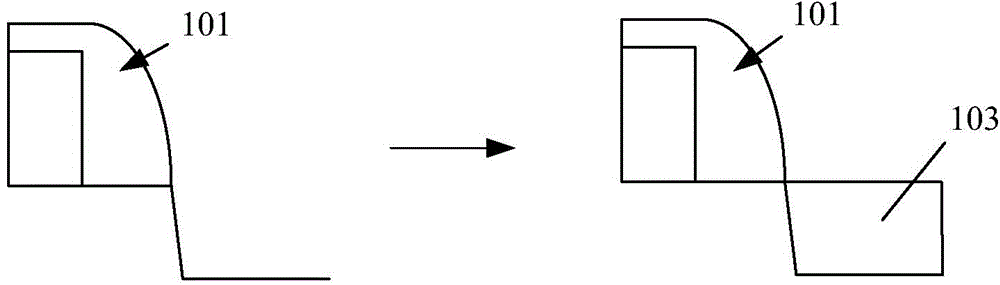
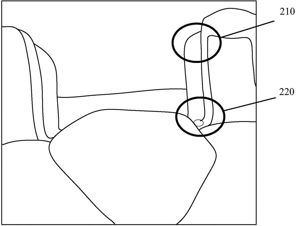
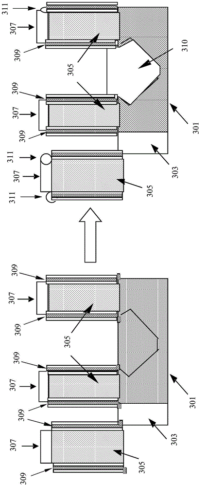
[0063] The present invention will be described in detail below with reference to the accompanying drawings. It should be understood that the following detailed description is merely exemplary in nature and is not intended to limit the embodiments of the subject matter or applications and the uses of these embodiments. As used herein, the word "exemplary" means "serving as an example, instance or illustration". Any implementation described herein as exemplary is not to be construed as necessarily preferred or superior over other implementations. Furthermore, there is no intention to be bound by any expressed or implied theory presented in the preceding technical field, background, brief summary or the following detailed description.

[0064] The terms "first," "second," "third," "fourth," etc., if any, in the description and claims are used to distinguish between similar elements and not necessarily to Describe a specific sequence or chronological order. It is to be understo...


PUM


Abstract

The invention discloses a method for forming embedded silicon germanium. The method comprises the following steps: providing a front-end device structure, wherein the front-end device structure comprises a semiconductor substrate and a gate structure arranged on the semiconductor substrate; depositing a carbon-doped silicon nitride layer on the surface of the front-end device structure; forming a silicon nitride film on the surface of the carbon-doped silicon nitride layer; carrying out photoetching and etching process, and forming sunken areas in the positions where a source electrode and a drain electrode are to be formed in the semiconductor substrate; and epitaxially growing the embedded silicon germanium in the sunken areas.

Description

technical field [0001] The present invention generally relates to semiconductor manufacturing processes, and more particularly to a method for forming embedded silicon germanium. Background technique [0002] At present, the main factor affecting the performance of field effect transistors is the mobility of carriers, where the mobility of carriers will affect the magnitude of the current in the channel. The reduction in carrier mobility in field-effect transistors not only reduces the switching speed of the transistor, but also reduces the difference in resistance between on and off. Therefore, in the development of complementary metal-oxide-semiconductor field-effect transistors (CMOS), effectively improving carrier mobility has always been one of the key points in transistor structure design. [0003] Conventionally, P-type metal-oxide-semiconductor field-effect transistors (PMOS) and N-type metal-oxide-semiconductor field-effect transistors (NMOS) are processed separate...

Claims


Application Information

Patent Timeline
IPC IPC(8): H01L21/336
Inventor 何有丰
Owner SEMICON MFG INT (SHANGHAI) CORP
Why Eureka
Try Eureka