
Preparation method for flexible carbon-nanotube field effect transistor

A technology of field-effect transistors and carbon nanotubes, applied in nanotechnology, nanotechnology, nanotechnology for materials and surface science, etc., can solve the problems of high manufacturing cost and low output of flexible carbon nanotube field-effect transistors, Achieve the effect of broad market application value

Inactive Publication Date: 2016-02-03
SHANGHAI INTEGRATED CIRCUIT RES & DEV CENT +1
View PDF4 Cites 7 Cited by
  • Summary
  • Abstract
  • Description
  • Claims
  • Application Information

AI Technical Summary

Problems solved by technology

However, due to limited process conditions and manufacturing capabilities, the preparation cost of flexible carbon nanotube field effect transistors is high and the output is low. In order to obtain large-scale practical applications of flexible carbon nanotube field effect transistors, it is necessary to develop low-cost mass production technology

Method used


Image

  • Preparation method for flexible carbon-nanotube field effect transistor
  • Preparation method for flexible carbon-nanotube field effect transistor
  • Preparation method for flexible carbon-nanotube field effect transistor

Examples


Embodiment Construction

[0035] In order to make the purpose, technical solution and advantages of the present invention clearer, the following will further describe the implementation of the present invention in detail in conjunction with the accompanying drawings. Those skilled in the art can easily understand other advantages and effects of the present invention from the contents disclosed in this specification. The present invention can also be implemented or applied through other different specific implementation modes, and various modifications or changes can be made to the details in this specification based on different viewpoints and applications without departing from the spirit of the present invention.

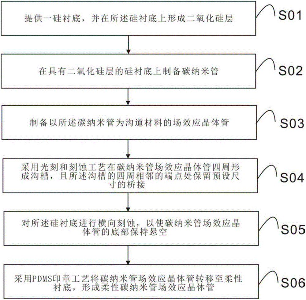
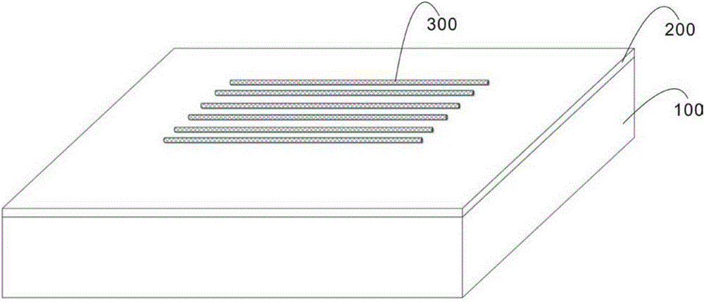
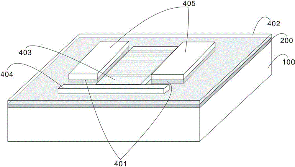
[0036] The above and other technical features and beneficial effects will be described in detail with reference to the embodiments and the accompanying drawings to the method for preparing a flexible carbon nanotube field effect transistor of the present invention. figure 1 It is a schemat...


PUM


Abstract

The invention discloses a preparation method for a flexible carbon-nanotube field effect transistor, and belongs to the field of semiconductor manufacture. A silicon substrate is provided, and carbon nanotubes are prepared on the silicon substrate; a field effect transistor taking the carbon nanotube as channel materials is prepared; trenches are formed in the periphery of the carbon-nanotube field effect transistor, and bridging of preset size is reserved in the adjacent end points of the trenches; the silicon substrate is etched horizontally, so that the bottom of the carbon-nanotube field effect transistor is suspended; and a PDMS stamping technology is used to transfer the carbon-nanotube field effect transistor to a flexible substrate to form the flexible carbon-nanotube field effect transistor. Mainstream preparation technologies of the high-performance carbon-nanotube transistor are combined, large-scale production of the flexible carbon-nanotube field effect transistors is realized by integrating the flexible packaging technology, and the market and application values of the method are high.

Description

technical field [0001] The invention belongs to the technical field of semiconductor manufacturing, and relates to a method for preparing a flexible carbon nanotube field effect transistor. Background technique [0002] In recent years, with the rapid development of flexible display technology and smart wearable products, flexible electronics has received more and more attention, and research on flexible field effect transistors (Field Effect Transistor, FET) has gradually become a hot topic. The fabrication process of flexible transistors is mainly based on organic semiconductor materials, or low-temperature polysilicon process. Although organic semiconductor materials have good flexibility and low process cost, their low carrier mobility greatly limits the improvement of device performance. At the same time, organic semiconductor materials are also extremely vulnerable to oxygen and humidity. , which leads to serious problems in the reliability of the device. In addition...

Claims


Application Information

Patent Timeline
IPC IPC(8): H01L21/336H01L29/16H01L29/78H01L29/06B82Y30/00B82Y40/00
CPCH01L29/66477B82Y30/00B82Y40/00H01L29/0673H01L29/16H01L29/78
Inventor 郭奥胡少坚周伟
Owner SHANGHAI INTEGRATED CIRCUIT RES & DEV CENT
Learn More