Package apparatus and manufacturing method thereof

A technology for packaging devices and manufacturing methods, which is applied in the fields of printed circuit manufacturing, semiconductor/solid-state device manufacturing, and printed circuits. It can solve problems such as expensive substrates, lack of industrial advantages, and restrictions on substrates with high-density wiring, so as to improve production. ability, shorten the center distance, and the effect of wide line width

Inactive Publication Date: 2016-02-10
PHOENIX PIONEER TECH
View PDF4 Cites 0 Cited by
  • Summary
  • Abstract
  • Description
  • Claims
  • Application Information

AI Technical Summary

Problems solved by technology

[0004] The above-mentioned traditional glass fiber substrate packaging structure 10 can only form the circular conductive column layer 120 with circular via holes by using the physical mechanism of mechanical drilling or laser drilling. However, the circular conductive column layer 120 has a larger The cross-sectional area will cause certain restrictions on the production of substrates with high-density wiring, making the cost of substrates too expensive to compete with industrial advantages

Method used


Image

  • Package apparatus and manufacturing method thereof
  • Package apparatus and manufacturing method thereof
  • Package apparatus and manufacturing method thereof

Examples


Embodiment Construction

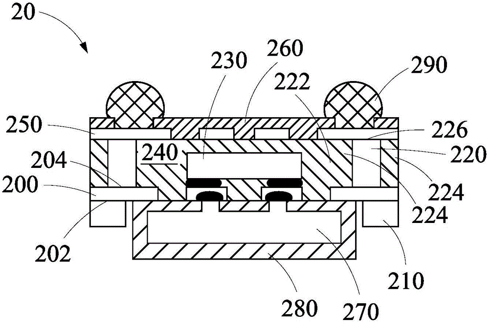
[0069] figure 2 It is a schematic diagram of a packaging device in a preferred embodiment of the present invention. The packaging device 20 includes a first wire layer 200, a metal layer 210, a first conductive column layer 220, an internal connection element 230, a first mold compound layer 240, a second wire layer 250 and a solder mask Layer 260, but not limited thereto.

[0070] The first wire layer 200 has a first surface 202 and a second surface 204 opposite to each other. In this embodiment, the first wire layer 200 is formed by using electrolytic plating technology, but it is not limited thereto. The first wiring layer 200 may be a patterned wiring layer, which includes at least one wire or at least one chip seat, and the material of the first wiring layer 200 may be metal, such as copper. The metal layer 210 is disposed on the first surface 202 of the first wire layer 200 .

[0071] The first conductive column layer 220 is disposed on the second surface 204 of the...


PUM


Abstract

A package apparatus comprises a first wiring layer, a first conductive pillar layer, a first molding compound layer, a second wiring layer, and a protection layer. The first wiring layer has a first surface and a second surface that are arranged opposite to each other. The first conductive pillar layer is disposed on the second surface of the first wiring layer, whereas the first conductive pillar layer is a non-circular conductive pillar layer. The first molding compound layer is disposed within a specific portion of the first wiring layer and the first conductive pillar layer. The second wiring layer is disposed on the first molding compound layer and one end of the first conductive pillar layer. The protection layer is disposed on the first molding compound layer and the second wiring layer.

Description

technical field [0001] The invention relates to a packaging device and a manufacturing method thereof, in particular to a semiconductor packaging device and a manufacturing method thereof. Background technique [0002] In the new generation of electronic products, the constant pursuit of thinner, lighter and smaller products requires multi-functional and high-performance products. Therefore, integrated circuits (Integrated Circuit, IC) must accommodate more electronic components in a limited area to achieve high density and high performance. To meet the requirements of miniaturization, the electronics industry has developed a new packaging technology for this purpose. Electronic components are embedded in the substrate, which greatly reduces the volume of the structure and shortens the connection path between electronic components and the substrate. In addition, it can also use the build-up technology (Build-Up ) to increase the wiring area to meet the trend of thin, light, ...

Claims


Application Information

Patent Timeline
Patent Type & Authority Applications(China)
IPC IPC(8): H01L23/528H01L21/768
CPCH01L23/49816H01L23/49827H01L23/49838H01L21/486H01L23/5389H05K1/115H05K1/187H05K1/188H05K3/0014H05K3/0017H05K3/007H05K3/16H05K3/181H05K3/421H05K2201/0209H05K2201/09118H05K2201/09536H05K2201/09636H05K2201/09854H05K2203/025H05K2203/0369H05K2203/0723H05K2203/0733H05K2203/1461H05K2203/1469H01L2924/181H01L2224/16227H01L2224/97H01L2924/15311H05K3/284H05K2201/0162H05K2201/09563H05K2203/1316H01L2224/04105H01L2224/16145H01L2224/18H01L24/20H01L24/19H01L2924/00012H01L2224/81H01L2924/0001H01L24/00
Inventor 胡竹青许诗滨周鄂东
Owner PHOENIX PIONEER TECH
Why Eureka
Try Eureka