Packaging structure for battery management integrated circuit
A technology of battery management and integrated circuits, applied in circuits, electrical components, electric solid devices, etc., can solve problems such as complex process, complex packaging structure, and increased cost, and achieve the effects of shrinking packaging structure, saving plane area, and reducing costs
- Summary
- Abstract
- Description
- Claims
- Application Information
AI Technical Summary
Problems solved by technology
Method used
Image
Examples
Embodiment Construction
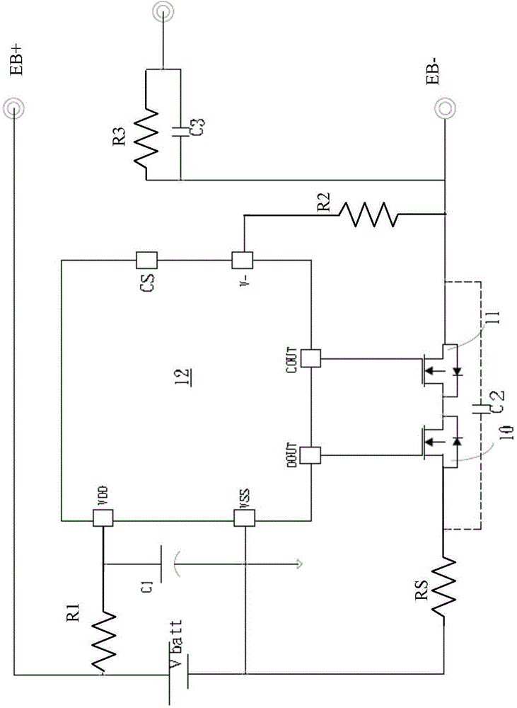
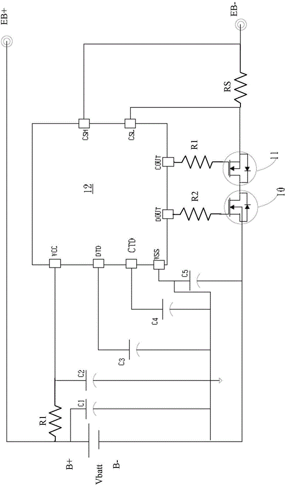
[0045] In summary, in the prior art, the separation of the battery management chip and the MOS transistor and the addition of external resistors and capacitors will make the entire package body have a considerable planar area: 21.9mm×3.55mm. However, the existing structure that is packaged into an integrated circuit has the problems of complicated process and high cost, which also makes its packaging not feasible. In addition, the resistance is enclosed inside. Heat dissipation is also a problem. The present invention therefore proposes a technique to overcome the above-mentioned problems. The detailed description is as follows:
[0046] In order to have a clearer understanding of the technical features, objectives and effects of the present invention, specific embodiments of the present invention will now be described with reference to the accompanying drawings.
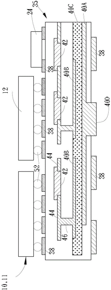
[0047] Such as image 3 According to an embodiment of the present invention, figure 1 The battery management chip s...
PUM
 Abstract
Description
Claims
Application Information
 - R&D
- Intellectual Property
- Life Sciences
- Materials
- Tech Scout
- Unparalleled Data Quality
- Higher Quality Content
- 60% Fewer Hallucinations
Browse by: Latest US Patents, China's latest patents, Technical Efficacy Thesaurus, Application Domain, Technology Topic, Popular Technical Reports.
© 2025 PatSnap. All rights reserved.Legal|Privacy policy|Modern Slavery Act Transparency Statement|Sitemap|About US| Contact US: help@patsnap.com


