Photon chip packaging structure based on grating interface, and manufacturing method for photon chip packaging structure

A photonic chip and packaging structure technology, applied in the direction of final product manufacturing, sustainable manufacturing/processing, climate sustainability, etc., can solve the problems of poor heat dissipation performance, complex process, poor performance of photonic chips, etc., to improve heat dissipation effect, Simple process, solve the effect of poor performance

Active Publication Date: 2016-02-17
NAT CENT FOR ADVANCED PACKAGING
View PDF5 Cites 8 Cited by
  • Summary
  • Abstract
  • Description
  • Claims
  • Application Information

AI Technical Summary

Problems solved by technology

[0005] The present application provides a photonic chip packaging structure and manufacturing method based on a grating interface, which solves the technical problems of poor performance, complex process and poor heat dissipation performance of the photonic chip caused by the integration technology in the prior art

Method used


Image

  • Photon chip packaging structure based on grating interface, and manufacturing method for photon chip packaging structure
  • Photon chip packaging structure based on grating interface, and manufacturing method for photon chip packaging structure
  • Photon chip packaging structure based on grating interface, and manufacturing method for photon chip packaging structure

Examples


Embodiment 1

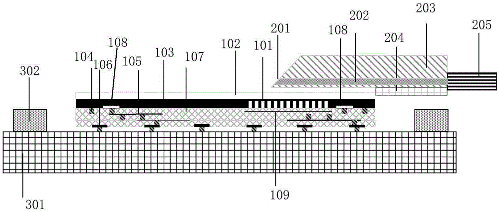
[0034] In order to solve the technical problems of poor performance of the photonic chip, complicated process and poor heat dissipation performance caused by the integration technology in the prior art, the present application provides a photonic chip packaging structure based on a grating interface. Such as figure 1 As shown, the photonic chip packaging structure based on the grating interface includes: an optoelectronic chip, an interconnection medium, a substrate 301 and an optical fiber coupling structure.

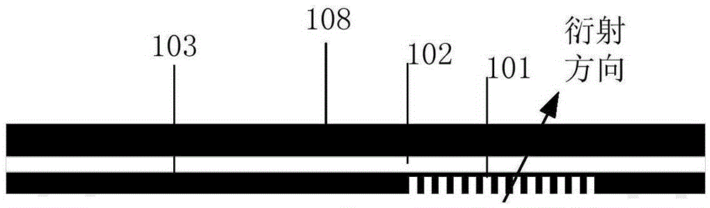
[0035] The optoelectronic chip includes an optoelectronic device (light modulator, detector, etc.) 108, a buried oxygen layer 102, a top silicon 103 and a back reflection grating 101 arranged on the top silicon 103.

[0036] The interconnection medium includes a multilayer dielectric layer 107 and an interconnection metal 105 arranged in the dielectric layer 107 for connecting the multilayer dielectric layer 107. Specifically, in this embodiment, the multi-layer dielectric ...

Embodiment 2

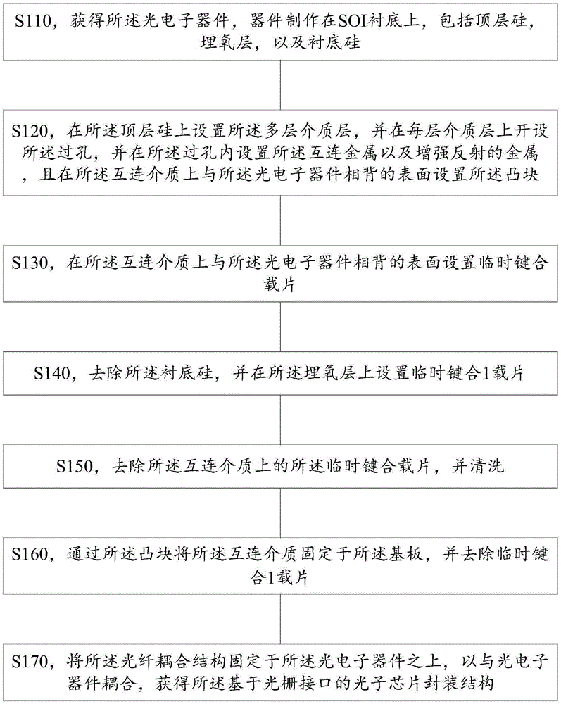
[0043] Based on the same inventive concept, the present application also provides a manufacturing method of a photonic chip packaging structure based on a grating interface. The manufacturing method is used to manufacture the photonic chip packaging structure based on a grating interface in the first embodiment. Such as figure 2 As shown, the manufacturing method includes the following steps:

[0044] Step S110, such as image 3 As shown, the optoelectronic chip is obtained, and a substrate silicon 108 is provided on the buried oxygen layer of the optoelectronic chip. The optoelectronic chip includes a buried oxygen layer 102, a top silicon 103, a back reflection grating 101 arranged on the top silicon 103, and an optoelectronic device.

[0045] Step S120, such as Figure 4-Figure 7 , A multi-layer dielectric layer 107 is provided on the top silicon 103, the via 104 is opened on each dielectric layer 107, and the interconnection metal 105 is provided in the via 104, and the enhanc...


PUM


Abstract

The invention discloses a photon chip packaging structure based on a grating interface, and a manufacturing method for the photon chip packaging structure. The structure is characterized in that the structure comprises a photoelectron chip; an interconnection medium, wherein the surface, opposite to the photoelectron chip, of the interconnection medium is provided with a convex block; and an optical fiber coupling structure which is fixed on the photoelectron chip and is used for coupling with a back reflection grating on the photoelectron chip. The structure is provided with a multi-layer medium, the multi-layer medium is provided with a via hole, and the interior of the via hole is provided with an interconnection metal. The structure employs the mature rewiring technology, is simple in technology, achieves the leading-out of input / output interfaces, and can flexibly distribute the input / output interfaces according to the subsequent integration needs, thereby achieving the interlayer connection, avoiding the employing of the silicon through hole technology, and protecting the performance of the photoelectron chip. In addition, the photoelectron chip is disposed at the same side of the interconnection medium and a substrate, thereby enabling the photoelectron chip to be connected in an inverted buckling manner, improving the transmission speed, and improving the heat-dissipation effect.

Description

Technical field [0001] The invention relates to the technical field of optoelectronic integration, in particular to a photonic chip packaging structure based on a grating interface and a manufacturing method thereof. Background technique [0002] Silicon-based photonic devices are compatible with complementary metal oxide semiconductor (CMOS) processes, are small in size, transparent in communication bands, large bandwidth, low latency, low energy consumption, low crosstalk and other advantages, and can be mixed or monolithically integrated with microelectronic chips. At present, silicon optoelectronic monolithic integrated circuits have achieved a high degree of integration, and modulators, and corresponding drivers, waveguide devices, detectors, and corresponding receiving and amplifying circuits can all be monolithically integrated. Since silicon itself is an indirect band gap semiconductor, the luminous efficiency has not reached the high-speed traffic demand, but many method...

Claims


Application Information

Patent Timeline
Patent Type & Authority Applications(China)
IPC IPC(8): H01L31/0203H01L31/18
CPCH01L31/0203Y02P70/50
Inventor 刘丰满曹立强郝虎
Owner NAT CENT FOR ADVANCED PACKAGING
Why Eureka
Try Eureka