Unlock instant, AI-driven research and patent intelligence for your innovation.
Preparation method for micro circuit flexible circuit board based on micro-nano imprinting technology
What is Al technical title?
Al technical title is built by PatSnap Al team. It summarizes the technical point description of the patent document.
A flexible circuit board, micro-nano technology, applied in the direction of printed circuit manufacturing, printed circuit, and the formation of electrical connection of printed components, can solve the problems of complex circuit board manufacturing process and high cost, reduce line width, not easy to scratch, The effect of simplifying the process flow
Active Publication Date: 2016-02-17
SHANGHAI LIANGZI HUIJING ELECTRONICS CO LTD
View PDF5 Cites 5 Cited by
Summary
Abstract
Description
Claims
Application Information
AI Technical Summary
This helps you quickly interpret patents by identifying the three key elements:
Problems solved by technology
Method used
Benefits of technology
Problems solved by technology
[0006] In view of the shortcomings of the prior art described above, the purpose of the present invention is to provide a method for preparing a micro-circuit flexible circuit board based on micro-nano imprinting technology, which is used to solve the problem of complicated circuit board manufacturing process and high cost in the prior art. The problem
Method used
Image
Click on the blue label to locate the original text in one second.
Reading with bidirectional positioning of images and text.
Examples
preparation example Construction
[0057] Such as Figure 1 to Figure 7 As shown, this embodiment provides a method for preparing a flexible circuit board with fine circuits based on micro-nano imprinting technology, which at least includes the following steps:
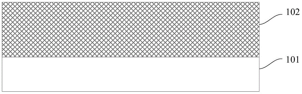
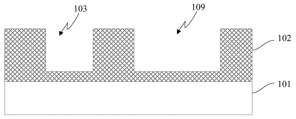
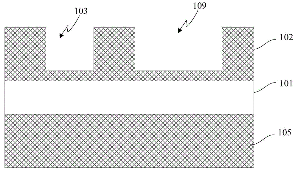
[0058] Such as Figure 1 ~ Figure 2 As shown, step 1) is performed first, providing a substrate 101, forming a first flexible material layer 102 on the first surface of the substrate 101, and forming a plurality of first groove structures 103 on the surface of the first flexible material layer 102 and several first hole structures 109;
[0059] As an example, the substrate 101 includes a PET flexible substrate and a PI flexible substrate. In this embodiment, the substrate is a PET flexible substrate.
[0060] As an example, the first flexible material layer 102 is a UV adhesive layer. In addition, it should be noted that UV glue is also called photosensitive glue and ultraviolet curing glue, which can be used as glue for paints, coatings, inks, etc. ...
Embodiment 2
[0076] Such as Figure 8 ~ Figure 10 As shown, this embodiment provides a method for preparing a flexible circuit board with fine circuits based on micro-nano imprinting technology, which at least includes the following steps:
[0077] Such as Figure 8 ~ Figure 9 As shown, step 1) is first performed, providing a substrate 201, forming a flexible material layer 202 on the surface of the substrate 201, and forming a plurality of groove structures 203 on the surface of the flexible material layer 202;
[0078] Such as Figure 10 As shown, then step 2) is performed to form conductive lines 204 in each groove structure 203 .
[0079] As an example, the groove structure has a depth of 30 microns to 50 microns, a width of 2 microns to 40 microns, and a cross-sectional shape of a trapezoidal structure with side walls having a draft angle of 1 to 3 degrees.
[0080] As an example, the groove structure is prepared by mold embossing.
PUM
Abstract
The invention provides a preparation method for a micro circuit flexible circuit board based on a micro-nano imprinting technology. The preparation method comprises the steps of forming a first flexible material layer and a second flexible material layer on the two surfaces of a substrate separately, forming a first groove structure and a first hole site structure, and forming a second groove structure and a second hole site structure separately; forming first conductive structures in each first groove structure and the first hole site structure; forming through holes in the substrate; and forming second conductive circuits in each second groove structure, the second hole site structure and the through holes to form a two-side interconnecting circuit. According to the preparation method for the micro circuit flexible circuit board based on the micro-nano imprinting technology, the combination between the conventional circuit board and the IC technology is realized, so that the application of micro electronic products on the flexible circuit boards is possible; the conductive circuits are embedded, so that the reliability of the circuits is greatly improved; the circuits prepared by a printing process or an electroplating process can form metallayers of different thicknesses in the internal and on the surface of the grooves; and in addition, a roll-to-roll technology is adopted, and pore formation is realized in the metal layer depositing process, so that the technology can be simplified and the cost can be reduced.
Description
technical field [0001] The invention relates to a method for preparing a circuit board, in particular to a method for preparing a micro-circuit flexible circuit board based on micro-nano imprinting technology. Background technique [0002] In recent years, with the explosive growth of information and communication electronic products and the continuous expansion of information network channels, the consumerelectronics industry has become one of the fastest growing industries in the world. The ever-changing electronic products are constantly developing in the direction of small size, light weight and complex functions. Printed circuit board (PCB), as an indispensable main part of electronic products, provides the interconnection of electrical signals and the support of electronic components. Especially flexible circuit board (FPC), is one of the industries with the most vigorous development momentum. Looking back at the FPC market in the past two years, it is found that th...
Claims
Application Information
Patent Timeline
Application Date:The date an application was filed.
Publication Date:The date a patent or application was officially published.
First Publication Date:The earliest publication date of a patent with the same application number.
Issue Date:Publication date of the patent grant document.
PCT Entry Date:The Entry date of PCT National Phase.
Estimated Expiry Date:The statutory expiry date of a patent right according to the Patent Law, and it is the longest term of protection that the patent right can achieve without the termination of the patent right due to other reasons(Term extension factor has been taken into account ).
Invalid Date:Actual expiry date is based on effective date or publication date of legal transaction data of invalid patent.

