Scan driving circuit and display device thereof

A technology for scanning driving circuits and driving circuits, applied in static indicators, instruments, etc., can solve the problems of increasing circuit power consumption, unfavorable for narrow frame design, increasing circuit signal lines and devices, etc. The effect of bezel design, signal lines and device reduction

Active Publication Date: 2016-02-24
WUHAN CHINA STAR OPTOELECTRONICS TECH CO LTD
View PDF8 Cites 36 Cited by
  • Summary
  • Abstract
  • Description
  • Claims
  • Application Information

AI Technical Summary

Problems solved by technology

The existence of U2D/D2U signal sources increases the signal lines and devices of the circuit, which is

Method used


Image

  • Scan driving circuit and display device thereof
  • Scan driving circuit and display device thereof
  • Scan driving circuit and display device thereof

Examples


Embodiment Construction

[0049] The implementation of the present invention will be described in detail below in conjunction with the accompanying drawings and examples, so that implementers of the present invention can fully understand how the present invention uses technical means to solve technical problems, and achieve the realization process of technical effects and according to the above-mentioned realization process The present invention is implemented concretely. It should be noted that, as long as there is no conflict, each embodiment and each feature in each embodiment of the present invention can be combined with each other, and the formed technical solutions are all within the protection scope of the present invention.

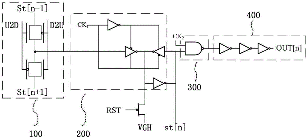
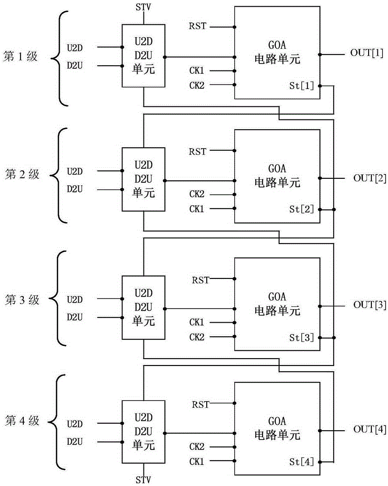
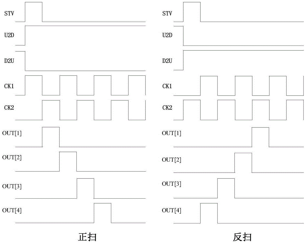
[0050] In the prior art, the GOA technology is usually used to drive the TFT liquid crystal display. That is to say, in the Array substrate manufacturing process, the Gate row scanning driving circuit that realizes the progressive scanning of the Gate is fabricated on the ...


PUM


Abstract

The invention discloses a scan driving circuit and a display device thereof. The scan driving circuit of the invention comprises an input unit, a latch unit, an NAND gate signal processing unit and an output buffering unit; and the input unit is configured to control the output of the input unit according to the different input combinations of last-level level transmission control signals, current-level level transmission control signals and next-level level transmission control signals of a current time sequence so as to output the current-level level transmission control signals of a next time sequence. Compared with the prior art, the scan driving circuit and the display device thereof of the invention can realize front and back scanning functions without relying on front and back scanning signals; the signal line and devices of the circuit are greatly reduced, and therefore, the design of a narrow frame can be benefitted, and the power dissipation of the circuit can be decreased; and the structure of existing substrate integrated circuit unit is not required to be modified, and the implementation difficulty of the scan driving circuit is low, the scan driving circuit has a high promotion value.

Description

technical field [0001] The invention relates to the field of liquid crystal display, in particular to a scanning driving circuit and a display device thereof. Background technique [0002] With the development of low-temperature polysilicon (LTPS) semiconductor thin film transistors, and due to the ultra-high carrier mobility characteristics of LTPS semiconductors, the corresponding panel peripheral integrated circuits have also become the focus of attention, and many people have invested in onboard systems ( SystemonPanel, SOP) related technology research, and gradually realize a variety of SOP. [0003] In the prior art, a thin-film transistor (Thin-filmtransistor, TFT) liquid crystal display is generally constructed using a substrate integration technology (Gate Driver On Array, GOA for short). That is, in the substrate (Array) manufacturing process, the Gate row scanning driving circuit that realizes the gate (Gate) progressive scanning is fabricated on the Array substr...

Claims


Application Information

Patent Timeline
IPC IPC(8): G09G3/36
Inventor 龚强
Owner WUHAN CHINA STAR OPTOELECTRONICS TECH CO LTD
Why Eureka
Try Eureka