Array substrate and manufacturing method therefor, display apparatus and mask plate

The technology of an array substrate and a manufacturing method, which is applied in the field of masks, can solve the problems of high manufacturing costs, complex manufacturing processes, and a large number of masks, and achieve the effect of reducing process costs and usage

Inactive Publication Date: 2016-02-24
BOE TECH GRP CO LTD +1
View PDF5 Cites 8 Cited by
  • Summary
  • Abstract
  • Description
  • Claims
  • Application Information

AI Technical Summary

Problems solved by technology

For top-gate thin film transistors, in the step of ion doping, the gate can be used as a mask for ion doping, but in order to prevent the influence of light on the active layer, it is necessary to form a light-shielding layer through another patterning process, so , the top-gate low-temperature polysilicon thin-film transistor requires at least five patterning processes, resulting in a large number of masks used; for the bottom-gate thin-film transistor, the light-shielding layer can be omitted, but it needs to be masked again when ion doping is performed. plate
It can be seen that the manufacturing process of low-temperature polysilicon thin film transistors in the prior art is relatively complicated, the number and frequency of masks used are large, and the manufacturing cost is relatively high.

Method used


Image

  • Array substrate and manufacturing method therefor, display apparatus and mask plate
  • Array substrate and manufacturing method therefor, display apparatus and mask plate
  • Array substrate and manufacturing method therefor, display apparatus and mask plate

Examples


Embodiment Construction

[0047] Specific embodiments of the present invention will be described in detail below in conjunction with the accompanying drawings. It should be understood that the specific embodiments described here are only used to illustrate and explain the present invention, and are not intended to limit the present invention.

[0048] As an aspect of the present invention, a method for manufacturing an array substrate is provided, including:

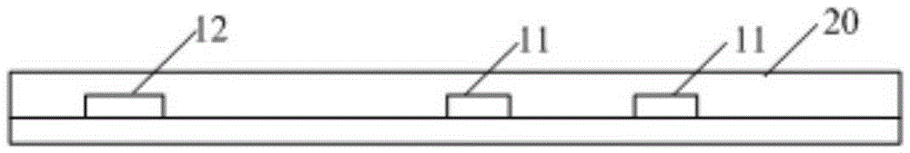
[0049] S1, forming a pattern including gate 11 and gate line 12, such as figure 1 shown;

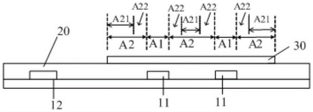
[0050] S2, forming an insulating layer 20, such as figure 2 shown;

[0051] S3, forming a pattern comprising the active layer 30, such as image 3 As shown, the region where the active layer is located includes a first region A1 corresponding to the gate and a second region A2 located on both sides of the first region A1;

[0052] S4. Form a mask pattern, the mask pattern includes a hollow part, a first part and a second part, the hollow part is used ...


PUM


Abstract

The invention provides an array substrate and a manufacturing method therefor, a display apparatus and a mask plate. The manufacturing method for the array substrate comprises the steps of S1, forming a pattern including a grid electrode and a grid line; S2, forming an insulating layer; S3, forming a pattern including an active layer, wherein the region where the active layer is positioned comprises a first region corresponding to the grid electrode and second regions positioned on the two sides of the first region; S4, forming a mask pattern, wherein the mask pattern comprises a hollow-out part, a first part and a second part; the thickness of the second part is less than that of the first part; S5, performing etching on the insulating layer to form a via hole for exposing a part of the grid line; and S6, performing ashing on the part, corresponding to the second regions, of the mask pattern so as to remove the part, corresponding to the second regions, of the mask pattern, and performing ion implantation in the active layer. According to the manufacturing method for the array substrate, the usage amount of the mask plates in the manufacturing technology can be reduced.

Description

technical field [0001] The present invention relates to the field of display technology, in particular to an array substrate and a manufacturing method thereof, a display device including the array substrate, and a mask plate. Background technique [0002] Low temperature poly-silicon (LTPS) thin film transistor liquid crystal display is different from the traditional amorphous silicon thin film transistor liquid crystal display. While improving the brightness of the display, it can also reduce the overall power consumption. In addition, the higher electron mobility can integrate part of the driving circuit on the glass substrate, reducing the cost of the driving circuit, and can also greatly improve the reliability of the liquid crystal display panel, thereby greatly reducing the manufacturing cost of the panel. Therefore, the low-temperature polysilicon thin film transistor liquid crystal display has gradually become a research hotspot. [0003] In the process of manufac...

Claims


Application Information

Patent Timeline
Patent Type & Authority Applications(China)
IPC IPC(8): H01L27/12H01L21/265H01L21/266
CPCH01L27/1288H01L21/02667H01L21/265H01L21/26513H01L21/266H01L27/1222H01L27/124H01L27/1274H01L29/66765H01L29/78621H01L27/1214H01L27/1259
Inventor 李付强
Owner BOE TECH GRP CO LTD
Why Eureka
Try Eureka