Array substrate and liquid crystal display device

An array substrate and display area technology, applied in instruments, semiconductor devices, optics, etc., can solve problems such as abnormal display of liquid crystal displays, and achieve the effect of reducing the impact

Active Publication Date: 2016-03-02
SHANGHAI TIANMA MICRO ELECTRONICS CO LTD +1
View PDF5 Cites 26 Cited by
  • Summary
  • Abstract
  • Description
  • Claims
  • Application Information

AI Technical Summary

Problems solved by technology

When opening the gate line G j , the gate lead S i with data line D i coupling between the data lines connected on the D i and gate line G j Thin film transistors have an impact, resulting in abnormal display of the liquid crystal display at low and medium gray levels, for example, the appearance of aircraft head graphics

Method used


Image

  • Array substrate and liquid crystal display device
  • Array substrate and liquid crystal display device
  • Array substrate and liquid crystal display device

Examples


Embodiment Construction

[0022] In order to make the above objects, features and advantages of the present invention more comprehensible, the present invention will be further described below in conjunction with the accompanying drawings and embodiments. It should be noted that in the following description, specific details are set forth in order to fully understand the present invention. However, the present invention can be implemented in many other ways than those described here, and those skilled in the art can make similar extensions without departing from the connotation of the present invention. Accordingly, the present invention is not limited to the specific embodiments disclosed below.

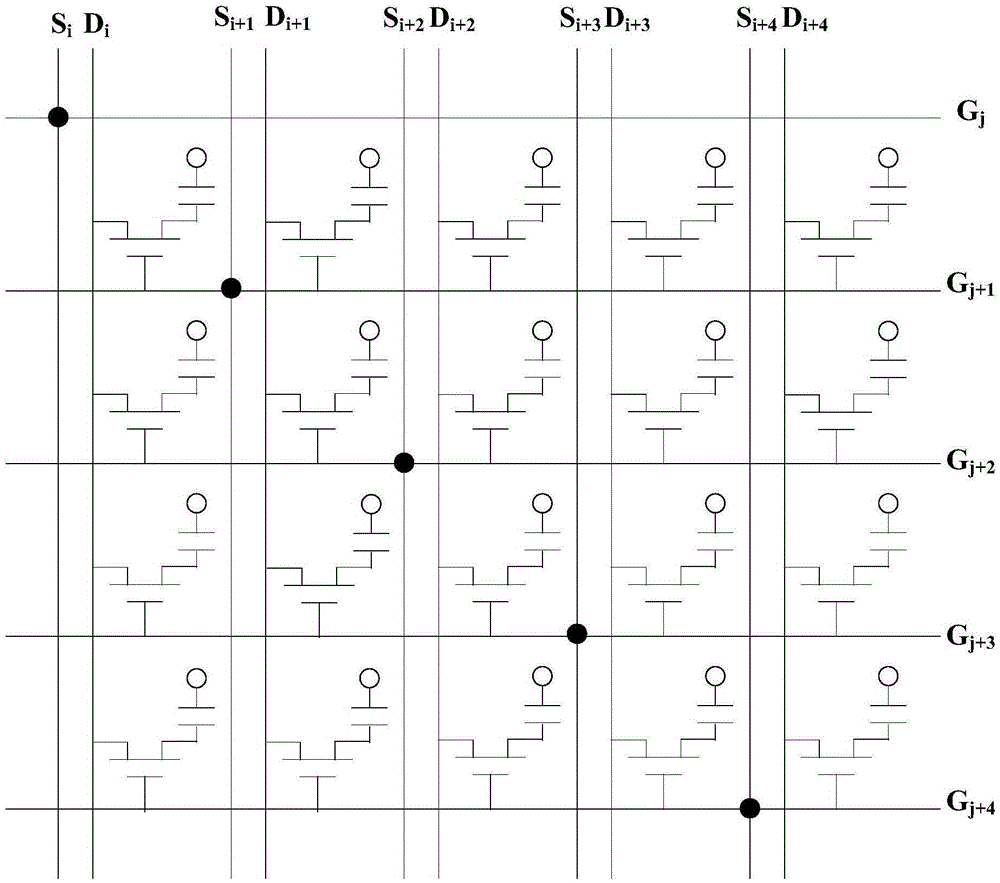
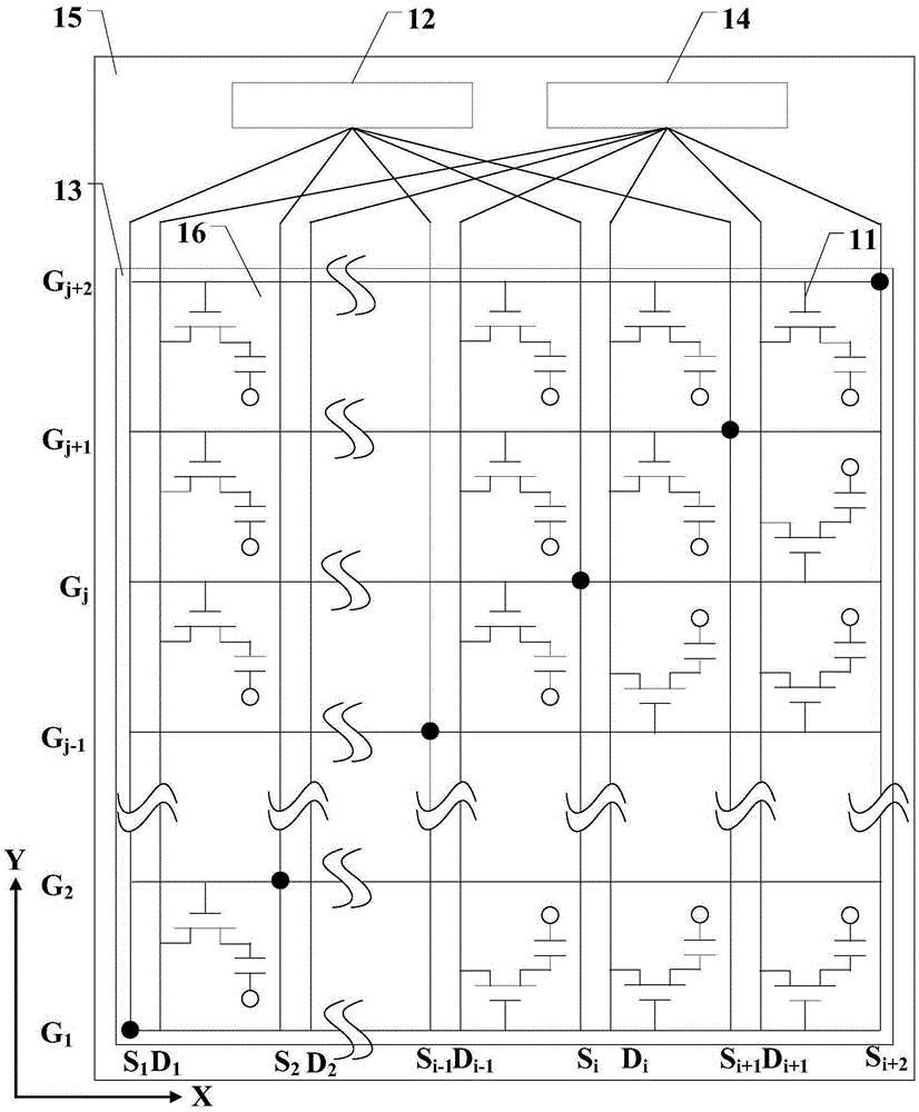
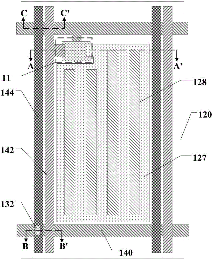
[0023] Please refer to Figure 2 to Figure 4c , figure 2 is a schematic structural view of an array substrate provided by an embodiment of the present invention, image 3 is the invention figure 2 A schematic diagram of a pixel structure, Figure 4a is the invention image 3 Sectional view at section...


PUM


Abstract

The invention discloses an array substrate and a liquid crystal display device comprising the same. The array substrate comprises a display area and a non-display area, wherein the display area comprises a plurality of pixel units, a plurality of grid lines, data lines and grid lead wires; two adjacent data lines and two adjacent grid lines are in a circle to form one pixel unit; each pixel unit comprises a thin film transistor and a pixel electrode; each grid lead wire is positioned between two corresponding adjacent pixel units; each grid line is connected with the corresponding grid lead line; the grid lead line in the i line is connected with the grid line in the j line, and the grid of the thin film transistor, connected with the data line in the i line, on the two sides of the grid line in the j line is connected with the grid line in the (j-1) line or the (j+1) line; i is an integer larger than 1; j is an integer larger than 1. According to the array substrate, the influence of the coupling of the grid lead lines and the data lines on the display pixels is reduced.

Description

technical field [0001] The invention relates to the display field, in particular to an array substrate and a liquid crystal display device including the array substrate. Background technique [0002] In the existing liquid crystal display, ASG (Amorphous Silicon Gate Driver, amorphous silicon gate driver) circuits are arranged on both sides of the display screen, occupying a large part of the frame area. As market demand changes, narrow bezels become the development trend of displays. In order to reduce the bezel or achieve no bezel, the ASG circuit can be placed under the display area (that is, the step area), and the ASG scanning The signal is connected to the gate line. figure 1 Schematic diagram of the structure of the array substrate after introducing gate leads in the prior art, as shown in the figure, the gate leads S i with data line D i set in parallel, each gate lead S i with a gate line G j connect. at the gate lead S i Gate line G j The connection between...

Claims


Application Information

Patent Timeline
Patent Type & Authority Applications(China)
IPC IPC(8): G02F1/1362G02F1/1368H01L27/12
CPCH01L27/124G02F1/136227G02F1/136286G02F1/1368
Inventor 李谷骏杨康毛琼琴
Owner SHANGHAI TIANMA MICRO ELECTRONICS CO LTD
Why Eureka
Try Eureka