LDMOS-SCR device with source-end embedded finger NMOS

A technology of LDMOS-SCR and devices, which is applied in the direction of electric solid-state devices, semiconductor devices, semiconductor/solid-state device components, etc., can solve the problems of insufficient anti-latch-up ability and low maintenance voltage, and increase the ESD current discharge capacity , enhance the resistance-capacitance coupling effect, and improve the effect of conduction uniformity

Active Publication Date: 2016-03-09
JIANGNAN UNIV
View PDF5 Cites 12 Cited by
  • Summary
  • Abstract
  • Description
  • Claims
  • Application Information

AI Technical Summary

Problems solved by technology

[0004] In view of the common problems of low maintenance voltage and insufficient anti-latch-up ability of the existing ESD protection devices with SCR structure, the present invention designs an LDMOS-SCR device with interdigitated NMOS embedded in the source end, which not only makes full use of the SCR The device is characte

Method used


Image

  • LDMOS-SCR device with source-end embedded finger NMOS
  • LDMOS-SCR device with source-end embedded finger NMOS
  • LDMOS-SCR device with source-end embedded finger NMOS

Examples


Embodiment Construction

[0025] Below in conjunction with accompanying drawing and specific embodiment the present invention will be described in further detail:

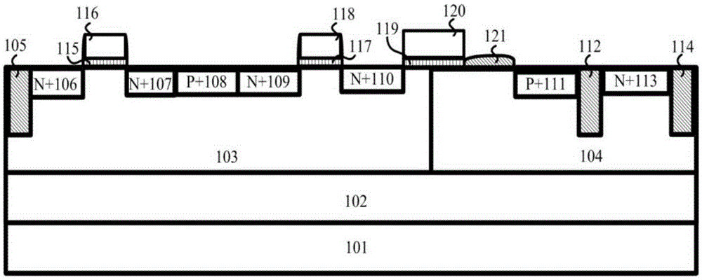
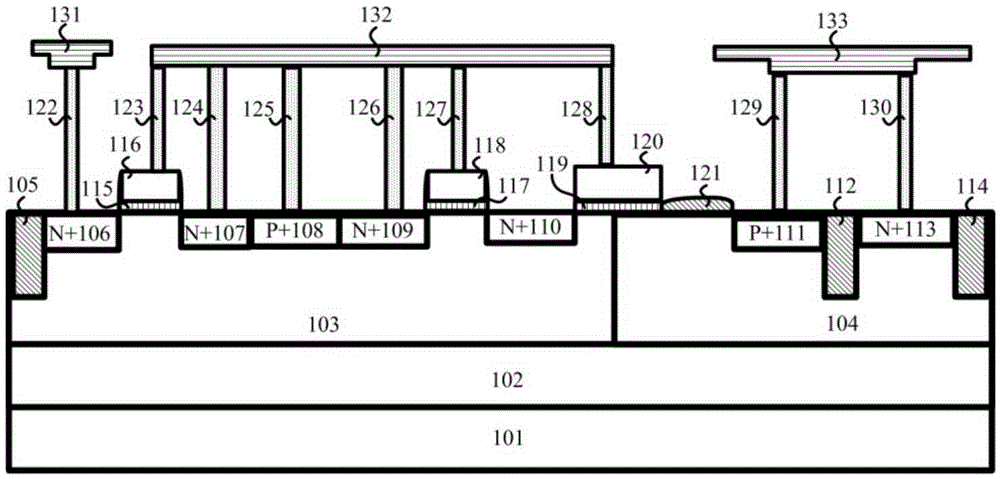
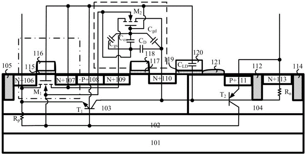
[0026] The example of the present invention designs an LDMOS-SCR device with interdigitated NMOS embedded in the source terminal, which not only utilizes the high-voltage resistance characteristics of LDMOS, but also utilizes the robustness of SCR strong ESD current. The interdigitated NMOS structure is embedded in the terminal design, and the resistance-capacitance coupling effect is formed by means of the source-side substrate parasitic resistance to improve the current conduction uniformity and turn-on speed of the device, enhance the ESD robustness of the device, and also increase the size of the device. the sustaining voltage.

[0027] Such as figure 1 The sectional view of the internal structure of the example device of the present invention shown, its main feature is: mainly by P substrate 101, P epitaxy 102, P well 103, N well 104,...


PUM


Abstract

The invention provides an LDMOS-SCR device with a source-end embedded finger NMOS, which can be applied to improving ESD protection reliability of an on-chip IC. The LDMOS-SCR device with the source-end embedded finger NMOS mainly comprises a P substrate, a P epitaxy, a P well, an N well, a first N+ injection region, a second N+ injection region, a first P+ injection region, a third N+ injection region, a fourth N+ injection region, a second P+ injection region, a fifth N+ injection region, a plurality of polysilicon gates, a plurality of thin gate oxides and a plurality of field oxide insulation regions. On one hand, the second P+ injection region, a third polysilicon gate, the fifth N+ injection region, the N well, the P well, the first P+ injection region, the first N+ injection region form a parasitical LDMOS-SCR current path, thereby reinforcing the ESD robustness of the LDMOS-SCR device; on the other hand, the first N+ injection region, a first polysilicon gate, a first thin gate oxide, the second N+ injection region, the first P+ injection region, the third N+ injection region, a second polysilicon gate, a second thin gate oxide and the fourth N+ injection region form the finger NMOS and a parasitic resistor, thereby forming a resistance-capacitance coupling effect; thereby, the maintaining voltage is increased.

Description

technical field [0001] The invention belongs to the field of electrostatic discharge protection of integrated circuits and relates to an ESD protection device, in particular to an ESD protection device with an LDMOS-SCR embedded with interdigitated NMOS at the source end, which can be used to improve the reliability of ESD protection of ICs on a chip . Background technique [0002] ESD (electrostatic discharge) is one of the important factors affecting the reliability of today's IC. Circuit dysfunction or gate oxide breakdown damage caused by ESD to ICs has attracted widespread attention in the industry. The damage phenomenon caused by ESD in IC is mainly manifested in the following aspects: dielectric breakdown caused by ESD in the semiconductor device, resulting in rupture of the oxide film; local overheating of the internal circuit caused by EOS (electrical overstress) or ESD in the IC, Lead to the melting of metal wires; in ESD protection devices, due to the low voltag...

Claims


Application Information

Patent Timeline
IPC IPC(8): H01L27/02H01L27/06H01L29/06H01L29/423H01L23/60
CPCH01L27/0248H01L23/60H01L27/0623H01L29/0649H01L29/0684H01L29/42356H01L29/42364
Inventor 梁海莲马艺珂顾晓峰丁盛
Owner JIANGNAN UNIV
Why Eureka
Try Eureka