OLED screen body and preparation method thereof

An electrode layer and substrate technology, applied in the field of OLED, can solve the problems of reducing efficiency and reducing the efficiency roll-off of the screen, and achieve the effects of suppressing the efficiency roll-off, improving the brightness, and improving the uniformity of light emission.

Active Publication Date: 2016-03-16
GUAN YEOLIGHT TECH CO LTD
View PDF4 Cites 2 Cited by
  • Summary
  • Abstract
  • Description
  • Claims
  • Application Information

AI Technical Summary

Problems solved by technology

[0004] Therefore, what the present invention is to solve is the problem that the efficiency of the existing OLED screen body will be greatly reduced with the increase of the current density, which is what we often call the efficiency roll-off (roll-off). The OLED screen that can achieve higher brightness adopts the method of limiting the size of the light-emi...

Method used


Image

  • OLED screen body and preparation method thereof
  • OLED screen body and preparation method thereof
  • OLED screen body and preparation method thereof

Examples


Embodiment 1

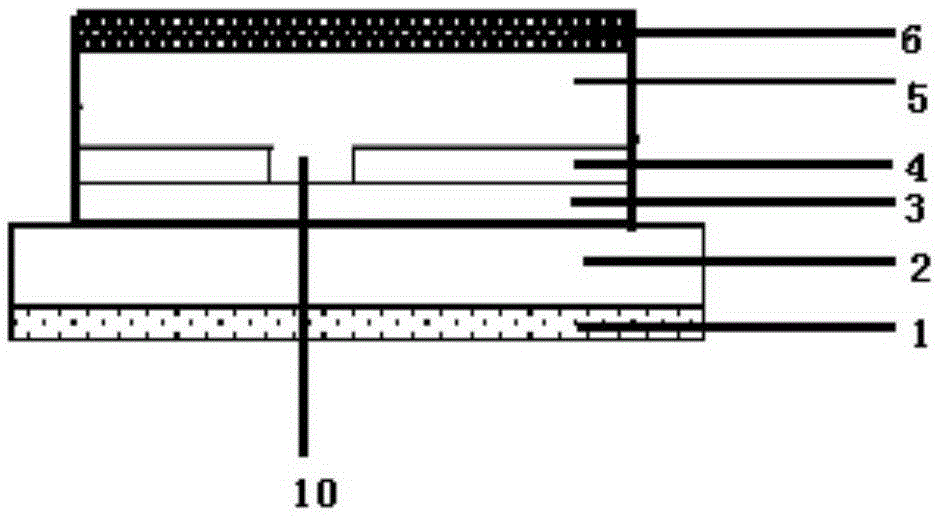
[0030] Embodiment 1 The scattering film layer 1 is arranged on the outside of the substrate

[0031] Such as figure 1 and Figure 4 As shown, a relatively bright OLED panel provided by the present invention includes a substrate 2 and a first electrode layer 3, an organic light-emitting layer 5 and a second electrode layer 6 are stacked on the substrate 2. An insulating film layer is arranged between an electrode layer 3 (anode) and the organic light-emitting layer 5, such as Figure 4 and Figure 5 As shown, the insulating film layer is etched to form parallel or criss-cross light-emitting regions 10, the width of each light-emitting region 10 is 5nm-500um, preferably 50nm-100um, between adjacent light-emitting regions 10 The width of the insulating material layer 4 is 10nm-100um. The thickness of the insulating film layer is 5-20nm. As other implementation manners, the insulating film layer may also be Figure 6 and Figure 7 As shown, its light-emitting area is a para...

Embodiment 2

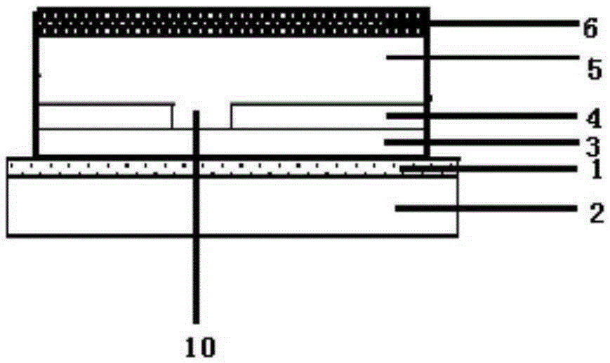
[0037] Embodiment 2 A scattering film layer 1 is arranged between the substrate and the first electrode layer

[0038] The structure of a relatively bright OLED screen body provided in this embodiment is the same as that in Embodiment 1, such as figure 2 As shown, the scattering film layer 1 is arranged between the substrate 2 and the first electrode layer 3 .

[0039]The preparation method is to arrange a scattering film layer 1 on the substrate 2, coat a layer of insulating film layer on the scattering film layer 1, and the width of the insulating material layer 4 between the adjacent light-emitting regions is 10nm-100um, and then pass the electron beam Photolithography technology carries out photoetching to etch out the light-emitting region 10, the width of the light-emitting region 10 is 5nm-500um, preferably the width is 50nm-100um, and then vapor-deposits the first electrode layer 3, the organic light-emitting layer 5 and the second electrode layer 6 ( cathode), packa...

Embodiment 3

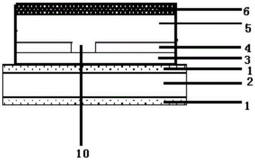
[0040] Embodiment 3 The scattering film layer 1 is respectively arranged on both sides of the substrate

[0041] The structure of a relatively bright OLED screen body provided in this embodiment is the same as that in Embodiment 1, such as image 3 As shown, the two sides of the substrate are respectively provided with scattering film layers 1, that is, one of the scattering film layers 1 is provided between the substrate 2 and the first electrode layer 3, and the other scattering film layer 1 is provided between the The side of the substrate away from the first electrode layer.

[0042] The preparation method is as follows: setting an upper scattering film layer 1 on the substrate 2, coating a layer of insulating film layer on the scattering film layer 1, and then performing photolithography to etch a light-emitting region 10 by electron beam lithography technology. The width of the light-emitting region 10 is 5nm-500um, the preferred width is 50nm-100um, the width of the in...


PUM

PropertyMeasurementUnit
Widthaaaaaaaaaa
Widthaaaaaaaaaa
Widthaaaaaaaaaa

Abstract

The invention provides an OLED screen body. The OLED screen body comprises a substrate, a first electrode layer, an organic light-emitting layer and a second electrode layer; the first electrode layer, the organic light-emitting layer and the second electrode layer are disposed on the substrate in an overlap manner; and an insulation film layer is disposed between the first electrode layer and the organic light-emitting layer, the insulation film layer forms parallel or criss-cross light-emitting regions through etching, and the width of each light-emitting region is 5nm to 500[mu]m. The sizes of the light-emitting regions between the first electrode layer and the organic light-emitting layer are limited through the insulation film layer, efficiency roll-off of the screen body is reduced, a scattering film layer is added, brightness of the screen body and light-emitting uniformity of the screen body are further improved, and then the OLED screen body having high brightness is prepared.

Description

technical field [0001] The invention relates to the technical field of OLEDs, in particular to a relatively bright OLED screen body. Background technique [0002] After nearly 30 years of development, organic electroluminescent devices (English full name OrganicLightEmittingDevice, referred to as OLED) as the next generation of lighting and display technology, has a wide color gamut, fast response, wide viewing angle, no pollution, high contrast, planarization And other advantages, has been applied to a certain extent in lighting and display. Such as figure 1 As shown, a typical organic electroluminescent device generally includes a transparent substrate, a transparent anode, a cathode, and an organic functional layer disposed between the two electrodes. [0003] Organic light-emitting diodes (Organic light-emitting diodes, OLED) have the characteristics of all-solid-state, flat-panel lighting, flexibility, and transparency, and have broad application prospects in lighting...

Claims


Application Information

Patent Timeline
IPC IPC(8): H01L51/52H01L27/32H01L51/56
CPCH10K59/00H10K50/854H10K2102/302H10K71/00
Inventor 朱映光谢静李曼张国辉胡永岚
Owner GUAN YEOLIGHT TECH CO LTD
Why Eureka
Try Eureka