Making technology of sensor packaging sheet

A manufacturing process and packaging sheet technology, applied in the field of sensor packaging sheet manufacturing process, can solve the problems of complex production process and the like

Inactive Publication Date: 2016-03-23
江西芯创光电有限公司
View PDF3 Cites 5 Cited by
  • Summary
  • Abstract
  • Description
  • Claims
  • Application Information

AI Technical Summary

Problems solved by technology

However, at present, when packaging photosensitive sheets, chips, and multiple substrates, multiple lamin

Method used


Image

  • Making technology of sensor packaging sheet
  • Making technology of sensor packaging sheet

Examples


Embodiment Construction

[0024] The present invention will be further described below in conjunction with the accompanying drawings and specific embodiments.

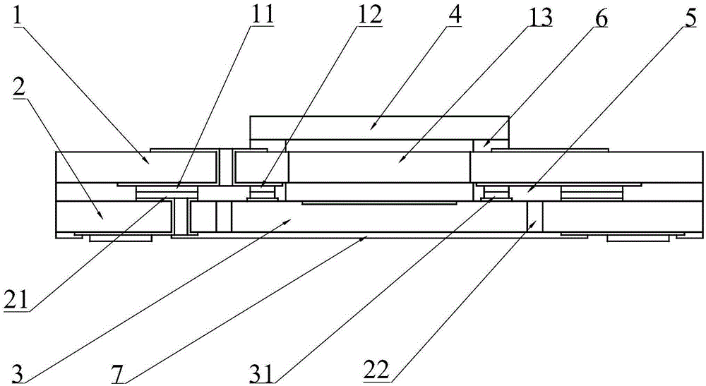
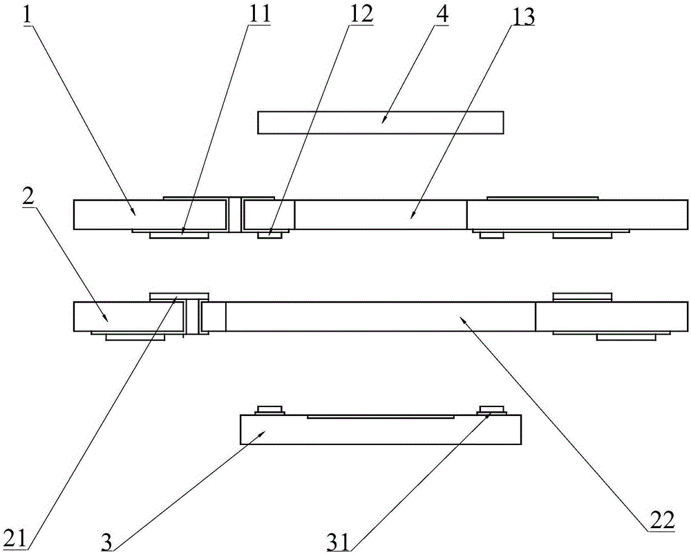
[0025] see figure 1 and figure 2 As shown, the technical solution of the present invention is to provide a manufacturing process of a sensor packaging sheet, which is characterized in that: the manufacturing process includes the following steps:

[0026] a) Select the upper substrate, the lower substrate and some chips and pre-process them;

[0027] b) coating the bottom surface of the upper substrate with a first adhesive material, and sequentially performing exposure, PEB and development on the first adhesive material;

[0028] c) bonding the bottom surface of the upper substrate to the top surface of the lower substrate;

[0029] d) Selecting a plurality of chips, the lower substrate is arranged with a number of placement holes, and the chips pass through the placement holes from the bottom surface of the lower substrate to the top surfa...


PUM


Abstract

The invention discloses a making technology of a sensor packaging sheet. By using the making technology, a process is simple, a degree of freedom is high and production precision is high too. A technical scheme is characterized by a) selecting an upper substrate, a lower substrate and several chips and carrying out pre-processing; b) coating a first adhesive material on a bottom surface of the upper substrate and successively carrying out exposure, PEB and development on the first adhesive material; c) carrying out alignment and attaching on the bottom surface of the upper substrate and a top surface of the lower substrate; d) selecting a plurality of chips, wherein the lower substrate is provided with several placing holes and the chips pass through the placing holes from a bottom surface of the lower substrate to the top surface and carry out alignment and attaching with the bottom surface of the upper substrate; e) carrying out whole plate lamination on the upper substrate, the lower substrate and the chips after attaching to obtain a semi-finished product A; f) attaching a top surface of the semi-finished product A to several optical filters and processing a reinforced layer on a bottom surface to obtain a semi-finished product B; g) carrying out solidification on the first adhesive material after the step e or the step f. The whole making technology has high precision and the process is simple.

Description

technical field [0001] The invention relates to the packaging field, and more specifically relates to a manufacturing process of a sensor packaging sheet. Background technique [0002] The packaging of most camera chips is based on the flip-chip technology, which has the following advantages: Compared with the traditional COB-based packaging, this method greatly improves the efficiency due to the removal of the wire-bond link; In addition, the package is packaged in a contiguous manner, and the efficiency can be further improved, and the production method of the substrate is similar to that of a general circuit board, which can effectively reduce equipment costs and material costs. However, at present, photosensitive sheets, chips, and multiple substrates need to be laminated multiple times when they are packaged, and after lamination, they need to be laminated, and the production process is complicated. Contents of the invention [0003] The technical problem to be solve...

Claims


Application Information

Patent Timeline
IPC IPC(8): H01L27/146
CPCH01L27/14687
Inventor 肖会华
Owner 江西芯创光电有限公司
Why Eureka
Try Eureka