Single-channel CMOS (Complementary Metal Oxide Semiconductor) image sensor and data transmission method thereof

An image sensor, single-channel technology, applied in the field of image sensors, to achieve the effect of reducing data flow, increasing frame rate, and reducing chip power consumption

Active Publication Date: 2016-03-23
SHANGHAI INTEGRATED CIRCUIT RES & DEV CENT +1
View PDF5 Cites 7 Cited by
  • Summary
  • Abstract
  • Description
  • Claims
  • Application Information

AI Technical Summary

Problems solved by technology

Some high-frame-rate CMOS image sensors usually use a single-channel data output architecture. However, for large-pixel CMOS image sensors with effective pixels above 16 million pixels, if the data flow capability required by full HD video streams is to be met, , the data flow of the data interface is also very considerable, which will bring great pressure to the high-speed data interface

Method used


Image

  • Single-channel CMOS (Complementary Metal Oxide Semiconductor) image sensor and data transmission method thereof
  • Single-channel CMOS (Complementary Metal Oxide Semiconductor) image sensor and data transmission method thereof
  • Single-channel CMOS (Complementary Metal Oxide Semiconductor) image sensor and data transmission method thereof

Examples


Embodiment 1

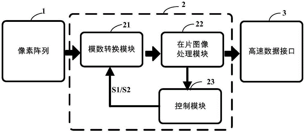
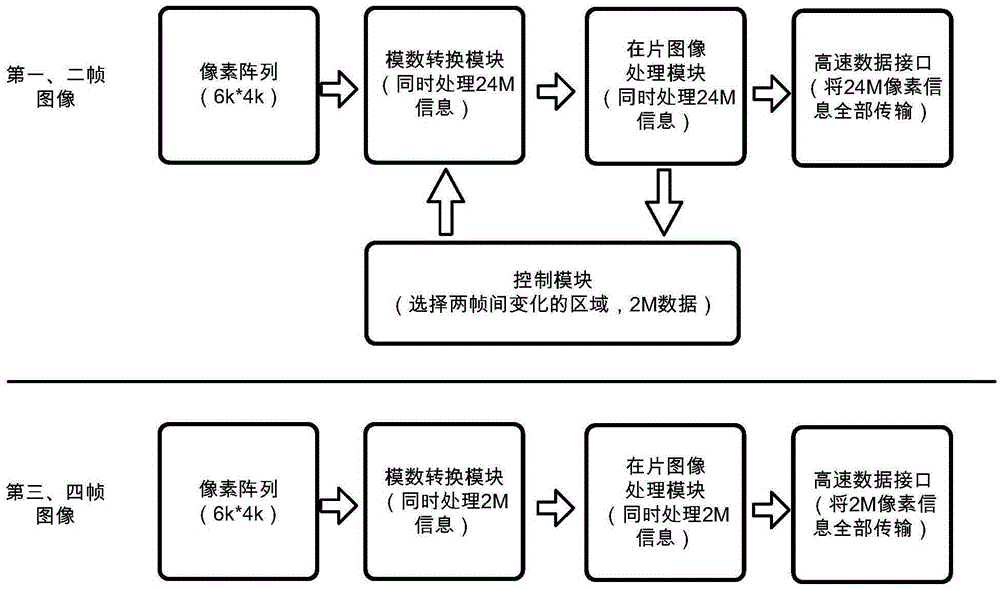
[0023] Please refer to figure 1 and figure 2 , the single-channel CMOS image sensor of this embodiment includes a pixel array 1 composed of a plurality of pixel units, a data processing unit 2 and a high-speed data interface 3 . Among them, the pixel unit is used to convert the optical signal into an analog electrical signal, and the data processing unit 2 is used to convert the analog electrical signal of the pixel unit into an image signal, and the converted image signal is output to the outside through the high-speed data interface 3 . The data processing unit 2 includes an analog-to-digital conversion module 21 , an on-slice image processing module 22 and a control module 23 . The analog-to-digital conversion module 21 can respond to the first control signal S1 or the second control signal S2 to perform the action of converting an analog signal into a digital signal. Specifically, the analog-to-digital conversion module 21 converts all pixels of the pixel array 1 to All...

Embodiment 2

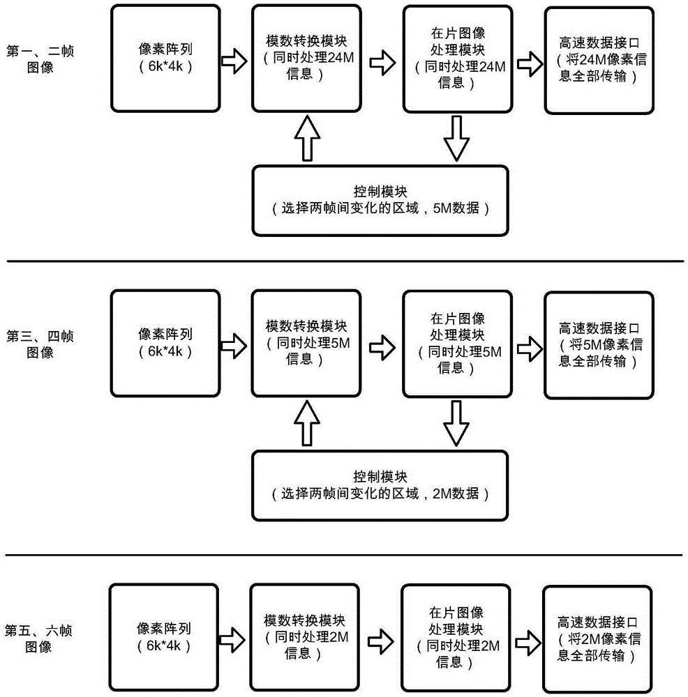
[0029] Please refer to figure 1 and image 3, the single-channel CMOS image sensor of this embodiment includes a pixel array 1 composed of a plurality of pixel units, a data processing unit 2 and a high-speed data interface 3 . Among them, the pixel unit is used to convert the optical signal into an analog electrical signal, and the data processing unit 2 is used to convert the analog electrical signal of the pixel unit into an image signal, and the converted image signal is output to the outside through the high-speed data interface 3 . The data processing unit 2 includes an analog-to-digital conversion module 21 , an on-slice image processing module 22 and a control module 23 . The analog-to-digital conversion module 21 can respond to the first control signal S1 or the second control signal S2 to perform the action of converting an analog signal into a digital signal. Specifically, the analog-to-digital conversion module 21 converts all pixels of the pixel array 1 to All t...


PUM


Abstract

The invention discloses a single-channel CMOS (Complementary Metal Oxide Semiconductor) image sensor, which comprises a pixel array formed by a plurality of pixel units and a data processing unit. The data processing unit comprises an analog-digital conversion module, an image processing module and a control module. The control module can recognize a region where two continuous frames of images have great changes and control the analog-digital conversion module to carry out analog-digital conversion on the image change region at the subsequent frame, so that the pressure from various aspects, such as on-chip analog digital signal conversion, on-chip image processing and high-speed data interface, can be greatly reduced.

Description

technical field [0001] The invention relates to the field of image sensors, in particular to a single-channel CMOS image sensor and a data transmission method thereof. Background technique [0002] Image sensors are an important part of digital cameras. According to the different components, it can be divided into two categories: CCD and CMOS. A prerequisite for the wide application of CMOS sensors is their higher sensitivity, shorter exposure time and shrinking pixel size. [0003] Generally speaking, the frame rate of a CMOS image sensor depends on the capability of the rear digital signal processor (DSP). Frames (fps) processing capability, which is sufficient to achieve the frame rate capabilities required for high-definition video streaming. [0004] But for some special applications, the video streaming frame rate of 30 or 60 frames per second is far from meeting its requirements. For example, for some scientific application cameras, it is usually necessary to shoo...

Claims


Application Information

Patent Timeline
Patent Type & Authority Applications(China)
IPC IPC(8): H04N5/374H04N5/3745
CPCH04N25/766H04N25/77
Inventor 李琛任铮刘浩蒋宇温建新
Owner SHANGHAI INTEGRATED CIRCUIT RES & DEV CENT
Why Eureka
Try Eureka