Wafer metal coating structure adapted to thinned back and toolings thereof

A metal coating and wafer technology, applied to the photographic process of the pattern surface, the original for photomechanical processing, optics, etc., can solve the problems of pollution, easily damaged surface of the wafer, etc., and achieve the elimination of unbalanced force , eliminate the risk of cracking and bending, solve the effects of breakage and staining

Active Publication Date: 2016-03-30
XIAN LIXIN PHOTOELECTRIC SCI & TECH
View PDF5 Cites 4 Cited by
  • Summary
  • Abstract
  • Description
  • Claims
  • Application Information

AI Technical Summary

Problems solved by technology

[0005] In order to solve the problem that the wafer is easily damaged and causes surface pollution during the wafer back thinning process, the present invention proposes a wafer metal coating structure

Method used


Image

  • Wafer metal coating structure adapted to thinned back and toolings thereof
  • Wafer metal coating structure adapted to thinned back and toolings thereof
  • Wafer metal coating structure adapted to thinned back and toolings thereof

Examples


Embodiment Construction

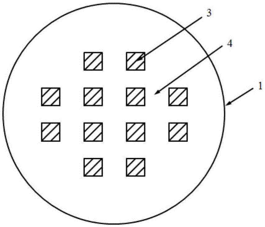
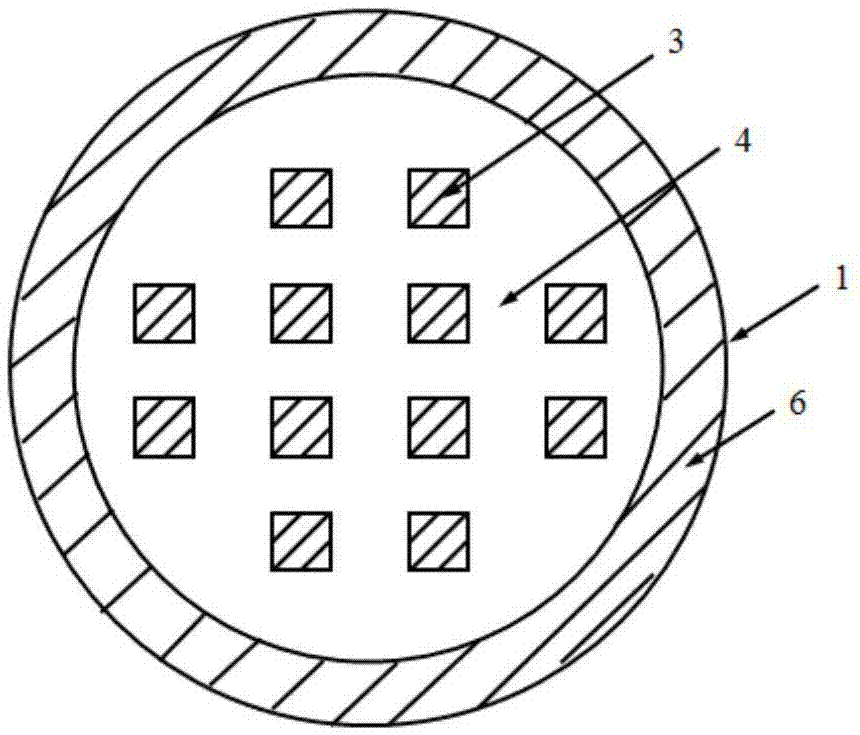
[0041] Such as figure 1 As shown, the metal is generally designed in the center of the wafer to meet the performance requirements of the device. Such as figure 2 As shown, the present invention specially designs and prepares a metal ring on the front side, which surrounds the edge of the wafer, eliminates the edge gap, improves the bonding effect between the front side of the wafer and the support carrier, and also solves the problem of abrasive particles entering the thinning grinding process. The problem.

[0042] Specific as Figure 4 As shown, a 5mm ring is designed from the edge of the wafer inward, and a layer of metal is prepared in this area at the same time when the wafer is operating the metal process. The same preparation process ensures that the thickness of the metal ring and the metal area are the same, so that there is no gap at the edge after the wafer is bonded to the support carrier, thereby ensuring that the wafer does not produce edge bending or cracks...


PUM

PropertyMeasurementUnit
widthaaaaaaaaaa

Abstract

The invention provides a wafer metal coating structure adapted to a thinned back and toolings (photoetched plates and wafer clamps) thereof. In the wafer metal coating structure, the middle part of the wafer metal coating is provided with a plurality of isolated metal zones used for realizing chip functions, and marked as chip active zones overall, and the difference from the existing technology is as follows: the peripheries of the chip active zones are provided with isolated metal ring belts, wherein the thickness of the metal ring belts is the same as that of the metal zones. When the wafer is thinned at the back, since metal exists at the wafer edge, the edge gap is eliminated, thus the problem that the edge stress of the wafer is uneven can be solved, and the risks of fracture and bending can be eliminated; meanwhile, since the edge gap is eliminated, a supporting carrier of the wafer edge can be totally fitted with the front, so that the probability that the thinned particles enter the wafer front can be eliminated and the problem of wafer surface contamination can be solved.

Description

technical field [0001] The invention relates to a wafer metal coating structure and corresponding tooling (lithography plate, wafer fixture). Background technique [0002] When wafers are used to prepare chips, the wafers need to be thinned for subsequent dicing and packaging and heat dissipation requirements. The usual practice is to use a support carrier to paste the front side of the wafer after the front side process of the wafer is completed, and then use abrasive particles with a hardness greater than that of the wafer for grinding and thinning on a thinning machine. After the wafer is thinned to the required thickness, the support carrier on the front side is removed, and the abrasive particles on the back side of the wafer are cleaned, so as to achieve the purpose of reducing the thickness of the wafer. [0003] When the wafer is working on the backside thinning process, the metal area on the front side of the wafer has a certain thickness. When the wafer is stuck o...

Claims


Application Information

Patent Timeline
Patent Type & Authority Applications(China)
IPC IPC(8): H01L21/02G03F1/00H01L21/687
CPCG03F1/68H01L21/02035H01L21/02697H01L21/687
Inventor 孙丞杨国文
Owner XIAN LIXIN PHOTOELECTRIC SCI & TECH
Why Eureka
Try Eureka