Semiconductor device, manufacturing method therefor, and electronic device

A technology for semiconductors and devices, applied in the field of semiconductor devices and their preparation, can solve the problems of difficult control of the height of metal gates, uneven height of metal gates, reduced device performance and yield, etc., to improve residual problems, improve uniformity, Improve the effect of control

Inactive Publication Date: 2016-03-30
SEMICON MFG INT (SHANGHAI) CORP
View PDF4 Cites 5 Cited by
  • Summary
  • Abstract
  • Description
  • Claims
  • Application Information

AI Technical Summary

Problems solved by technology

However, it is difficult to determine the end position of the planarization step, which makes it difficult to control the height of the metal gate, causing the problem of uneven height of the metal gate, which reduces the performance and yield of the device

Method used


Image

  • Semiconductor device, manufacturing method therefor, and electronic device
  • Semiconductor device, manufacturing method therefor, and electronic device
  • Semiconductor device, manufacturing method therefor, and electronic device

Examples


Embodiment 1

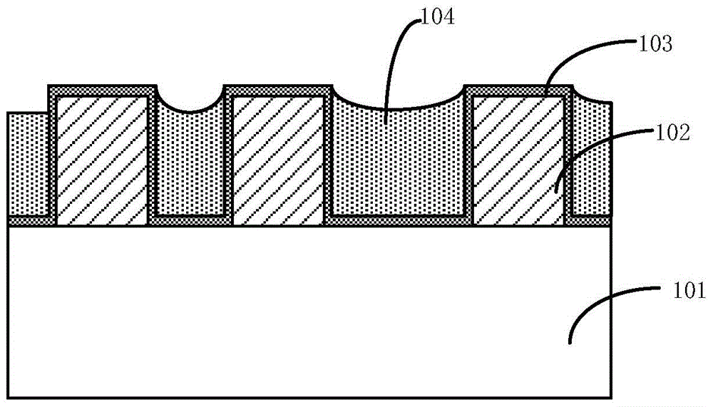
[0037] At present, the fabrication methods of semiconductor devices containing metal gates are as follows: figure 1 As shown, first a substrate 101 is provided, a dummy gate structure 102 is formed on the substrate, and then a spacer layer and / or a contact hole etch stop layer 103 is formed on the substrate 101 and the dummy gate structure 102, and Depositing a FCVD dielectric layer 104 by FCVD (fluid chemical vapor deposition) method on the spacer layer and / or contact hole etch stop layer 103, and then performing dry etching, wet etching and planarization on the FCVD dielectric layer, Wherein the surface of the FCVD dielectric layer 104 is severely recessed after planarization (such as figure 1 As shown), it affects the determination of the end point of the metal gate planarization in the subsequent process, so that the height of the metal gate is difficult to control, resulting in uneven height of the metal gate, which affects the performance and yield of the device.

[003...

Embodiment 2

[0087] The present invention also provides a semiconductor device, which is prepared by the method described in Embodiment 1. The height of the metal grid in the semiconductor device prepared by the method of the present invention is easier to control, and the height is more uniform, which improves the performance and yield of the semiconductor device.

Embodiment 3

[0089]The present invention also provides an electronic device, including the semiconductor device described in Embodiment 2. Wherein, the semiconductor device is the semiconductor device described in Embodiment 2, or the semiconductor device obtained according to the preparation method described in Embodiment 1.

[0090] The electronic device of this embodiment can be any electronic product or equipment such as mobile phone, tablet computer, notebook computer, netbook, game console, TV set, VCD, DVD, navigator, camera, video recorder, voice recorder, MP3, MP4, PSP, etc. , can also be any intermediate product including the semiconductor device. The electronic device according to the embodiment of the present invention has better performance due to the use of the above-mentioned semiconductor device.


PUM


Abstract

The invention relates to a semiconductor device, a manufacturing method therefor, and an electronic device. The method comprises the steps: providing a substrate, and forming a virtual grid, a gap wall layer and / or contact hole etching stop layer located on a side wall of the virtual grid, and an interlayer dielectric layer which covers the gap wall layer and / or contact hole etching stop layer; carrying out flattening from the interlayer dielectric layer to the virtual grid; carrying out the back etching of the gap wall layer and / or contact hole etching stop layer; removing the virtual grid and then forming a metal grid; and carrying out flattening from the metal grid to the gap wall layer and / or contact hole etching stop layer. The method is characterized in (1), improving the determination of a flattening end point signal of the metal grid, so as to improve the control of the height of the grid, and to improve the height uniformity of the metal grid; (2), improving a residue problem of the metal grid; (3), enlarging the technological window of the rear grid process of the metal grid.

Description

technical field [0001] The present invention relates to the field of semiconductors, in particular, the present invention relates to a semiconductor device, a preparation method thereof, and an electronic device. Background technique [0002] In the field of integrated circuit manufacturing, as the size of MOS transistors continues to shrink, the impact of the physical limits of devices is also increasing, and it becomes more difficult to scale down the feature size of devices. Among them, MOS transistors and their circuits The manufacturing field is prone to leakage problems from the gate to the substrate. [0003] The current method to solve the above problems is to replace the conventional polysilicon gate structure with high-K metal gates in semiconductor devices. At present, most of the formation methods of metal gates adopt the gate-last process. For example, a dummy gate is formed first, then an interlayer dielectric layer is deposited to cover the dummy gate, and fi...

Claims


Application Information

Patent Timeline
Patent Type & Authority Applications(China)
IPC IPC(8): H01L21/28H01L21/336
Inventor 曾以志赵杰
Owner SEMICON MFG INT (SHANGHAI) CORP
Why Eureka
Try Eureka