Method for forming semiconductor device
A semiconductor and device technology, applied in the field of semiconductor device formation, can solve problems such as failure to meet the development requirements of semiconductor devices, poor performance of semiconductor devices, etc., and achieve the effect of reducing performance and reducing adverse effects
- Summary
- Abstract
- Description
- Claims
- Application Information
AI Technical Summary
Problems solved by technology
Method used
Image

Examples
Embodiment Construction
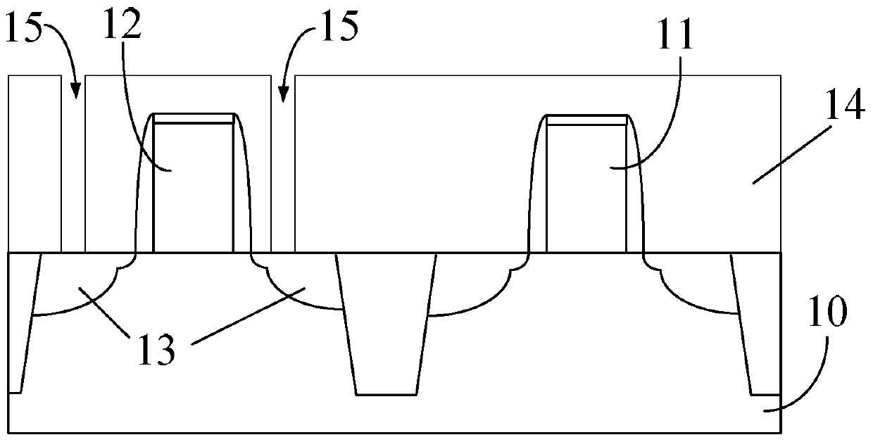
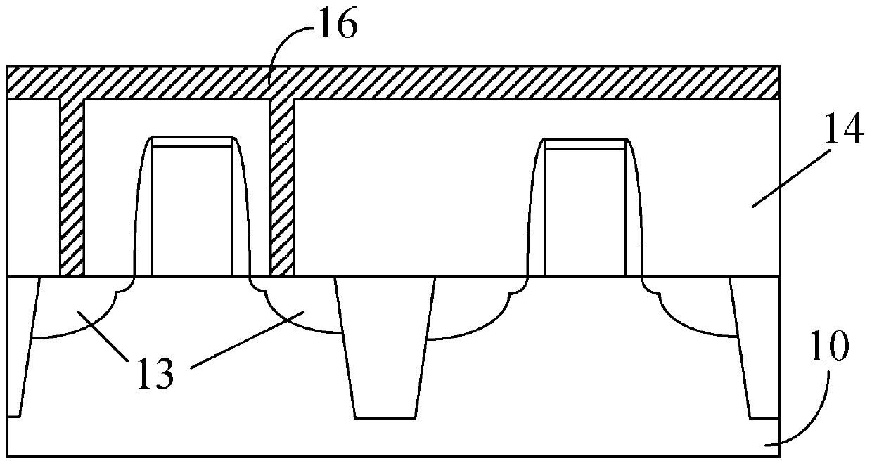
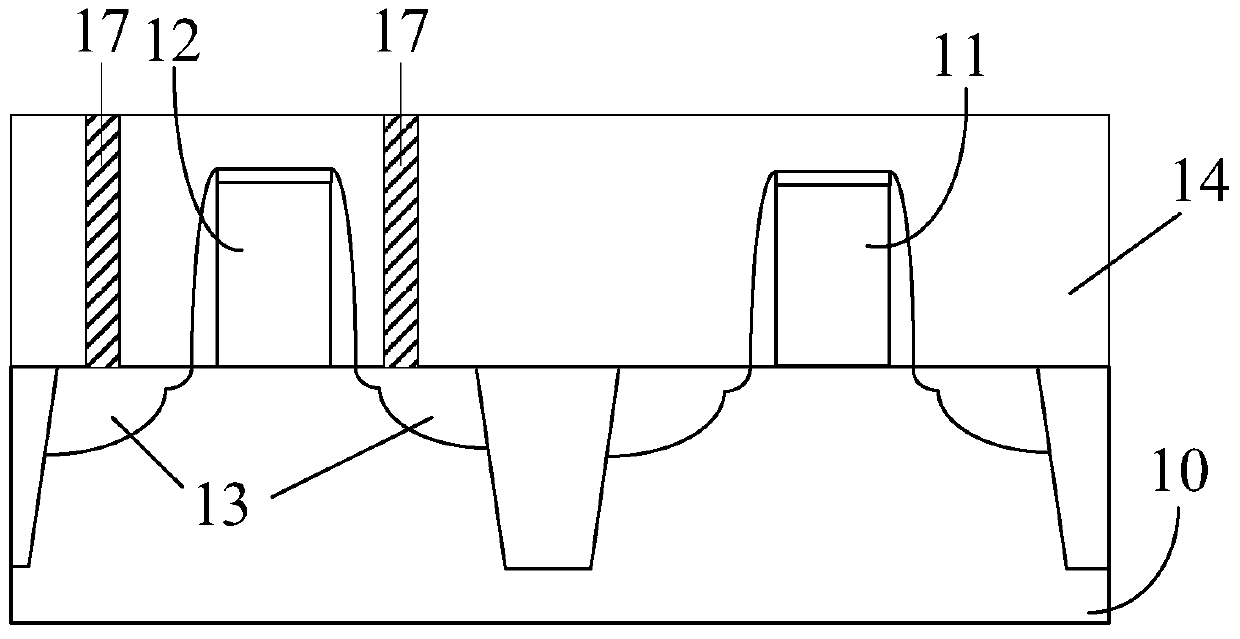
[0045] As mentioned in the background technology, the performance of the semiconductor device after the interconnection structure formed by the existing process cannot meet the needs, and the reason is analyzed: combined with reference Figure 1 to Figure 6 .
[0046] In the formation process of the existing interconnect structure, a first through hole 15 is formed in the first dielectric layer 14, and a first metal layer filling the first through hole 15 is formed on the first dielectric layer 14 After 16 , CMP is used to remove the redundant first metal layer 16 on the first dielectric layer 14 , so as to form a first conductive plug 17 in the first through hole 15 . Wherein, in the CMP process, after the polishing pad removes the first metal layer 16 on the first dielectric layer 14, it is also easy to remove the first dielectric layer 14 with a partial thickness, but the grinding rate based on the first conductive plug 17 is much lower than that of the first dielectric layer...
PUM
 Abstract
Description
Claims
Application Information
 - R&D
- Intellectual Property
- Life Sciences
- Materials
- Tech Scout
- Unparalleled Data Quality
- Higher Quality Content
- 60% Fewer Hallucinations
Browse by: Latest US Patents, China's latest patents, Technical Efficacy Thesaurus, Application Domain, Technology Topic, Popular Technical Reports.
© 2025 PatSnap. All rights reserved.Legal|Privacy policy|Modern Slavery Act Transparency Statement|Sitemap|About US| Contact US: help@patsnap.com