
Sensor and assembly methods thereof

An assembly method and a sensor technology, which are applied in the field of sensing, can solve problems affecting reliability, large height difference between lead plate pads and chip pads, and lead wire lengthening, etc., to achieve improved reliability, simple and compact structure, and shortened length Effect

Active Publication Date: 2016-03-30
48TH RES INST OF CHINA ELECTRONICS TECH GROUP CORP
View PDF6 Cites 2 Cited by
  • Summary
  • Abstract
  • Description
  • Claims
  • Application Information

AI Technical Summary

Problems solved by technology

like figure 1 As shown, in order to ensure the strength and electrical performance of the solder joints, the solder joints will protrude from the surface of the lead plate by 0.8mm to 1.5mm, and the solder joints are between the lead plate and the chip, that is, the height difference between the lead plate and the chip is at least 0.8mm, resulting in The height difference between the lead plate pad and the chip pad is large, and the lead wire becomes longer, which affects reliability

Method used


Image

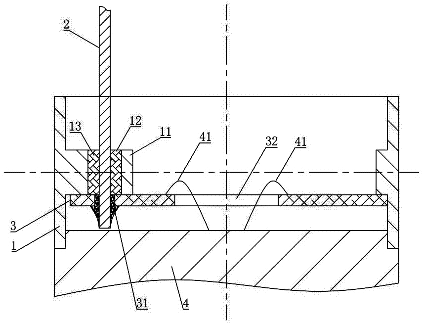
  • Sensor and assembly methods thereof
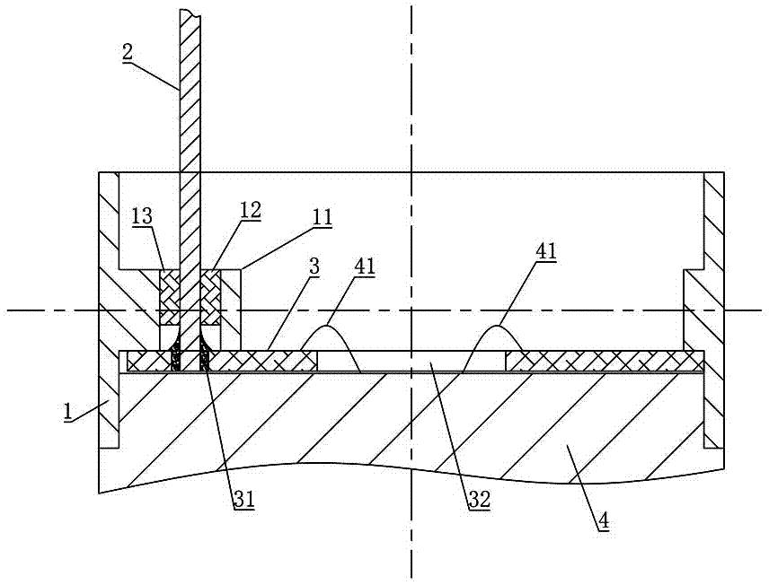
  • Sensor and assembly methods thereof
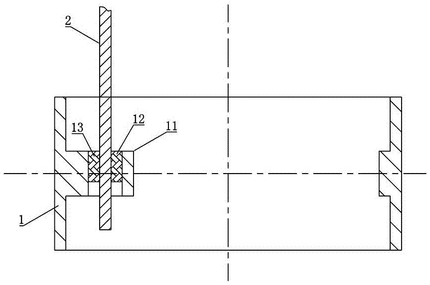
  • Sensor and assembly methods thereof

Examples


Embodiment 1

[0033] Such as Figure 3 to Figure 5 As shown, the assembly method of the sensor of the embodiment of the present invention includes the following steps:

[0034] S01, start, fill the upper part of the lead pin hole 12 on the protruding ring 11 of the inner wall of the lead bracket 1 with an insulating layer 13 and fix the lead pin 2 in the lead pin hole 12;

[0035] S02. Assemble the lead plate 3 to the inside of the lead frame 1 and contact the lower surface of the lead frame 1. At this time, the lower part of the lead pin 2 is inserted into the welding hole 31 of the lead plate 3 and its lower end surface is in contact with the lower surface of the lead plate 3. The surface is even, and then the lead plate 3 is welded to the lead pin 2, and the solder joint is extended to the lower part of the lead pin hole 12. Specifically, spot welding can be used to weld the lower surface of the lead plate 3, and the solder liquid It is left to the upper part of the lead plate 3, that i...

Embodiment 2

[0039] The assembly method of the sensor of the embodiment of the present invention comprises the following steps:

[0040] S01, start, insert the lower part of the lead pin 2 into the welding hole 31 of the lead plate 3, then weld the lead plate 3 and the lead pin 2 on the upper surface of the lead plate 3, and ensure that the lower end surface of the lead pin 2 is in contact with the lead wire The lower surface of the board 3 is flush. This method can directly weld the lead pin 2 to the lead board 3 above the lead board 3, and the solder joints will stay directly above the lead board 3 to ensure that the lower surface of the lead board 3 is flush. ;

[0041] S02. Assemble the lead pin 2 and the lead plate 3 into the lead frame 1, the lead plate 3 is in contact with the lower surface of the protruding ring 11, the lead pin 2 passes through the through hole on the protruding ring 11 on the inner wall of the lead frame 1, and The hole is filled with an insulating layer 13 to f...


PUM


Abstract

The invention discloses a sensor, which comprises a lead pin, a lead bracket, a lead board and a chip, wherein a convex ring is arranged on the inner wall of the lead bracket; a lead pin hole is formed in the convex ring; the upper part of the lead pin hole is filled with an insulating layer; the lead pin passes through the lead pin hole, is inserted into a welding hole and is welded; the lower end surface of the lead pin is flush with the lower surface of the lead plate; the chip is in contact with the lower surface of the lead board; and the lead of the chip passes through a lead hole and is welded with the upper surface of the lead board. The invention further discloses an assembly method of the sensor. The method comprises the following steps: firstly, fixing the lead pin on the lead bracket; and then welding the lead pin and the lead board and ensuring that the lower surface of the lead board is flush. The invention further discloses another assembly method, which comprises the following steps: welding the lead pin and the lead board and then fixing the lead pin in the lead pin hole, and simultaneously ensuring that the lead pin does not extend out of the lower surface of the lead board. The sensor and the assembly methods thereof disclosed by the invention have the advantages of being simple and compact in structure, short in lead, high in working reliability and the like.

Description

technical field [0001] The invention mainly relates to the field of sensor technology, in particular to a sensor and an assembly method thereof. Background technique [0002] With the wide application of sensor technology, the reliability of the sensor is required to be higher and higher, and the lead technology of the chip is the key to the reliability of the sensor. [0003] In the common lead method, the lead plate is welded on the pins of the lead frame, and then the lead frame and the chip are assembled together. like figure 1 As shown, in order to ensure the strength and electrical performance of the solder joints, the solder joints will protrude from the surface of the lead plate by 0.8mm to 1.5mm, and the solder joints are between the lead plate and the chip, that is, the height difference between the lead plate and the chip is at least 0.8mm, resulting in The height difference between the lead plate pad and the chip pad is large, and the lead wire becomes longer, ...

Claims


Application Information

Patent Timeline
Patent Type & Authority Applications(China)
IPC IPC(8): H01L23/488
CPCH01L2224/48091H01L2924/00014H01L23/488H01L24/63
Inventor 蓝镇立何峰寻骈臻谢明颜志红
Owner 48TH RES INST OF CHINA ELECTRONICS TECH GROUP CORP
Learn More