

Dynamic random access memory and its manufacturing method
A technology of dynamic random access and manufacturing methods, applied in semiconductor/solid-state device manufacturing, transistors, electrical components, etc., can solve problems such as difficult readout margins, achieve the effect of improving readout margins and reducing leakage
- Summary
- Abstract
- Description
- Claims
- Application Information
AI Technical Summary
Problems solved by technology
Method used
Image

Examples
Embodiment Construction
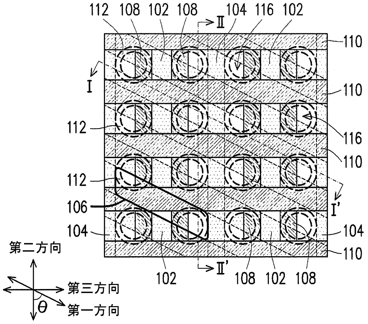
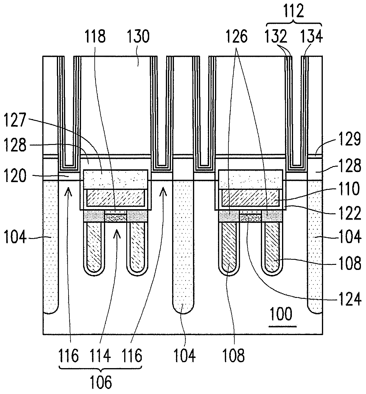
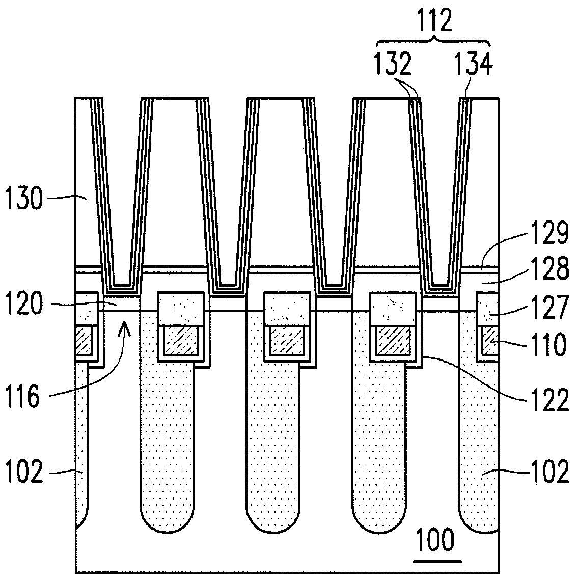
[0050] Figure 1A is a top view of a DRAM according to the first embodiment of the present invention. Figure 1B yes Figure 1A The cross-sectional schematic diagram of the I-I' line segment. Figure 1C yes Figure 1A A schematic cross-sectional view of the II-II' line segment.
[0051] Please also refer to Figure 1A , 1B Compared with 1C, the DRAM of this embodiment includes a silicon substrate 100, a first isolation trench structure 102, a second isolation trench structure 104, an active region 106, a buried word line 108 located in the silicon substrate 100, and a Buried bit lines 110 and capacitors 112 in the silicon substrate 100 . In order to clearly illustrate the circuit of the dynamic random access memory, Figure 1A Only the above components are shown in , other structures are visible Figure 1B and Figure 1C sectional view.
[0052] In the first embodiment, the first isolation trench structures 102 are arranged in parallel in the silicon substrate 100 along t...
PUM
 Abstract
Description
Claims
Application Information