
SMD component processing method

A technology for patch components and processing methods, which is applied in the direction of electrical components, semiconductor/solid-state device manufacturing, circuits, etc., and can solve the problems of easy short-circuiting, small electrode spacing, and contamination of the sides.

Active Publication Date: 2018-07-31
NANTONG FUJITSU MICROELECTRONICS
View PDF6 Cites 0 Cited by
  • Summary
  • Abstract
  • Description
  • Claims
  • Application Information

AI Technical Summary

Problems solved by technology

[0002] In the prior art, the electrode part of the patch component usually has no protective layer, and the distance between the electrodes is small, and the short circuit between the adjacent devices is very easy to occur after the device is mounted.
In addition, the electrodes need to be connected by solder balls, and the solder balls generally use tin balls, and the tin will "climb" along the electrodes and stain the sides, making it prone to short circuits

Method used

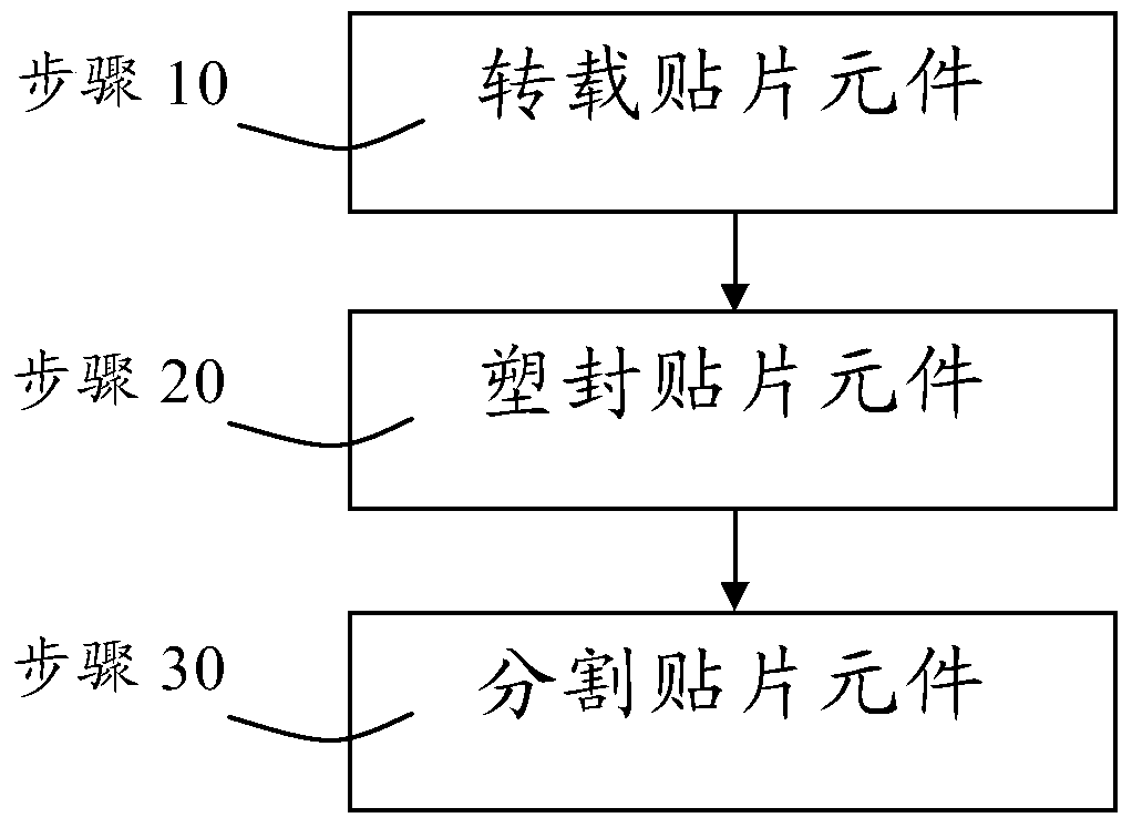
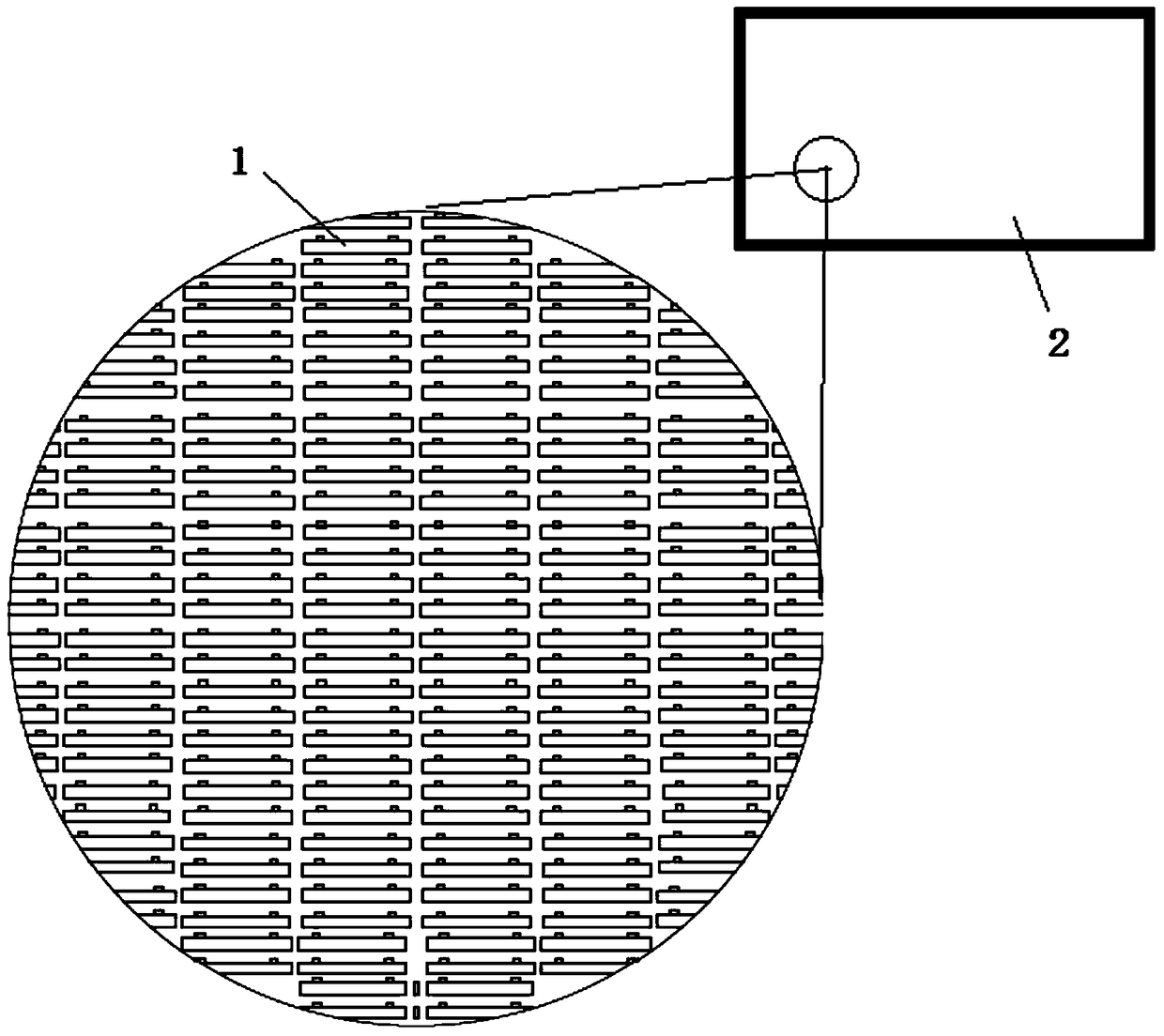

Image

  • SMD component processing method
  • SMD component processing method
  • SMD component processing method

Examples


Embodiment 1

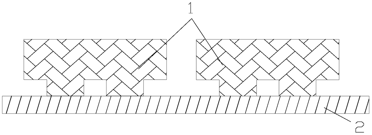
[0022] There are protruding electrodes 11 on the patch component, and when the patch component is transferred to the carrier 2 , the electrode 11 faces the carrying surface of the carrier 2 . Such as Figure 3A and 3B shown. That is, with the surface where the electrode 11 is located as the front, the surface of the patch component is placed on the carrier 2 facing the carrying surface, and the protruding electrodes 11 are supported on the carrying surface.

[0023] When placed in this way, a plastic sealing method may be: inject the plastic sealant 3 from above the patch component in a direction perpendicular to the bearing surface, and plastic seal the patch component. This can prevent the plastic sealant 3 from completely sealing the electrodes 11 , and there is no need to subsequently remove the plastic sealant 3 to expose the electrodes 11 .

[0024] Another way of molding is: injecting the molding compound 3 from the gap between the patch component and the bearing sur...

Embodiment 2

[0028] The patch component has a protruding electrode 11 , and when the patch component is transferred to the carrier 2 , the electrode 11 faces away from the carrying surface of the carrier 2 . Such as Figure 6 shown. That is to say, the surface where the electrode 11 is located is defined as the front side, and the opposite side is defined as the back side, and the back side of the chip component faces the carrying surface and is placed on the carrier.

[0029] In this way of placement, the molding compound 3 is injected from around the electrodes 11 during injection molding to seal the patch components. formed as Figure 7 structure shown. Injecting from all around can avoid completely encapsulating the electrode 11 into the injection molding glue.

[0030] The above two embodiments are optional two ways for processing and preparing patch components. The patch components processed in the above-mentioned manner of the present invention can avoid short circuits between t...


PUM


Abstract

The present application discloses a method for processing patch components. The patch components are transferred to a carrier, and the patch components are evenly arranged; the patch components transferred to the carrier are plastic-sealed to form a plastic package. There are electrodes on the patch element, and the pin ends of the electrodes are exposed from the surface of the plastic package; the patch component is separated from the carrier, and the plastic package is divided to form a single patch with a plastic package structure element. The SMD components are plastic-sealed, and the pin ends of the electrodes are exposed for connection. The plastic package protects the SMD components and avoids the short circuit caused by the close distance between the SMD components and adjacent devices. At the same time, when the solder balls are connected, the tin in the solder balls pollutes the electrodes to cause a short circuit.

Description

technical field [0001] The present disclosure generally relates to the field of semiconductors, and in particular relates to chip components in the semiconductor manufacturing process, especially a processing method for chip components. Background technique [0002] In the prior art, the electrode part of the chip component usually has no protective layer, and the distance between the electrodes is small, and short circuit between adjacent devices is very easy to occur after the device is mounted. Moreover, the electrodes need to be connected through solder balls when connecting, and the solder balls generally use tin balls, and the tin will "climb" along the electrodes and stain the sides, making it prone to short circuits. Contents of the invention [0003] In view of the above-mentioned defects or deficiencies in the prior art, it is desired to provide a method for processing patch components, which is to transfer the patch components to the carrier, and the patch compo...

Claims


Application Information

Patent Timeline
Patent Type & Authority Patents(China)
IPC IPC(8): H01L21/50H01L21/56
Inventor 沈海军
Owner NANTONG FUJITSU MICROELECTRONICS
Learn More