Wafer lifting assembly, and mechanical arm used for placing wafer on or taking wafer from wafer lifting assembly

A manipulator and wafer technology, applied in the field of microelectronics, can solve problems such as electrostatic chuck sticking, incomplete electrostatic discharge, tilting, etc., and achieve the effect of solving damaged wafers

Inactive Publication Date: 2016-04-06
BEIJING NAURA MICROELECTRONICS EQUIP CO LTD
View PDF4 Cites 2 Cited by
  • Summary
  • Abstract
  • Description
  • Claims
  • Application Information

AI Technical Summary

Problems solved by technology

The traditional substrate material Si (silicon) is easier to be adsorbed. However, with the continuous expansion and deepening of the MEMS application field, more and more substrate materials are introduced into ICP etching, including SiC (silicon carbide), SiO2 ( Silicon oxide), etc., these materials have high requirements on the electrostatic adsorption capacity of the chuck o

Method used


Image

  • Wafer lifting assembly, and mechanical arm used for placing wafer on or taking wafer from wafer lifting assembly
  • Wafer lifting assembly, and mechanical arm used for placing wafer on or taking wafer from wafer lifting assembly
  • Wafer lifting assembly, and mechanical arm used for placing wafer on or taking wafer from wafer lifting assembly

Examples


Embodiment Construction

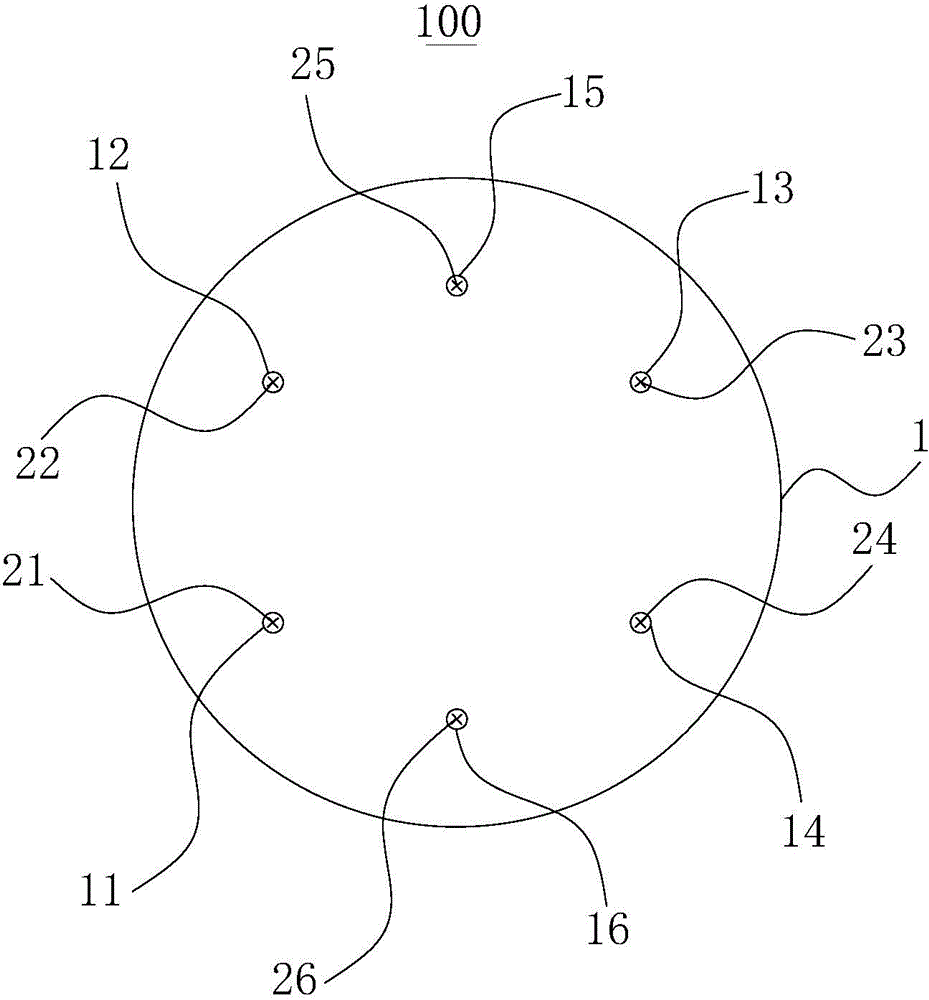
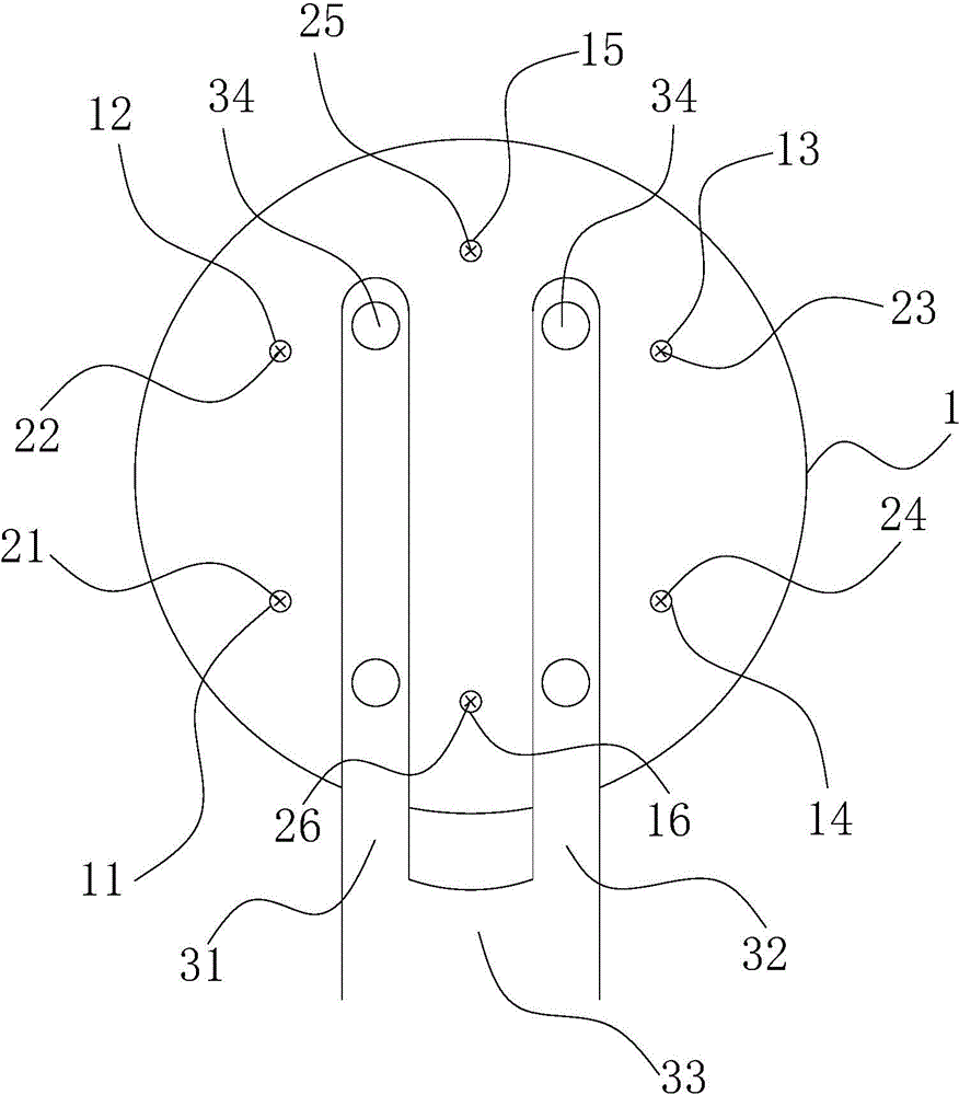
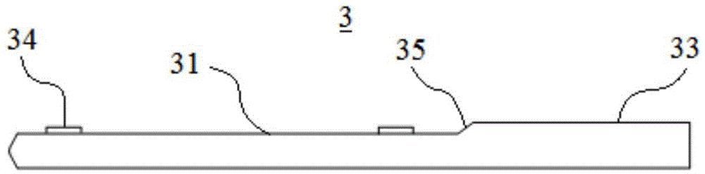
[0033] Embodiments of the present invention are described in detail below, examples of which are shown in the drawings, wherein the same or similar reference numerals designate the same or similar elements or elements having the same or similar functions throughout. The embodiments described below by referring to the figures are exemplary only for explaining the present invention and should not be construed as limiting the present invention.

[0034] In describing the present invention, it is to be understood that the terms "centre", "length", "width", "upper", "lower", "left", "right", "vertical", "horizontal", The orientations or positional relationships indicated by "top", "bottom", "inner", "outer", etc. are based on the orientations or positional relationships shown in the drawings, and are only for the convenience of describing the present invention and simplifying the description, rather than indicating or implying References to devices or elements must have a particula...


PUM

PropertyMeasurementUnit
Widthaaaaaaaaaa

Abstract

The invention discloses a wafer lifting assembly, and a mechanical arm used for placing a wafer on or taking a wafer from the wafer lifting assembly. The wafer lifting assembly comprises a chuck and lifting pins from the first to the sixth, wherein the chuck is used for supporting a wafer, through holes from the first to the sixth are formed in the chuck, the through holes from the first to the fourth are formed at four corners of a first rectangle, the center of the first rectangle coincides with the center of the chuck, and the fifth through hole and the sixth through hole are formed in a midperpendicular of a group of parallel edges of the first rectangle and are formed outside the first rectangle and symmetric to each other relative to the center of the first rectangle; the lifting pins from the first to the sixth are in one-to-one correspondence with the through holes from the first to the sixth, the lifting pins can move relative to the chuck, and pass through the corresponding through holes from the first to the sixth for lifting the wafer supported on the chuck. According to the wafer lifting assembly provided by the invention, the wafer inclining situation cannot occur, thereby solving the problems that the wafer inclination is prone to occur after wafer bonding and the wafer is damaged during the wafer taking process by the mechanical arm.

Description

technical field [0001] The invention relates to the technical field of microelectronics, in particular to a wafer lifting assembly and a manipulator for picking and placing wafers from the wafer lifting assembly. Background technique [0002] As MEMS (Micro-Electro-MechanicalSystem, micro-electromechanical system) devices and MEMS systems are more and more widely used in the fields of automobiles and consumer electronics, dry plasma etching equipment is gradually introduced into the field of MEMS processing. [0003] It is pointed out in the related art that during the ICP (Inductive Coupled Plasma, Inductively Coupled Plasma) etching process, more and more ICP etching machines use electrostatic chucks to adsorb the substrate. The traditional substrate material Si (silicon) is easier to be adsorbed. However, with the continuous expansion and deepening of the MEMS application field, more and more substrate materials are introduced into ICP etching, including SiC (silicon carb...

Claims


Application Information

Patent Timeline
IPC IPC(8): H01L21/677H01L21/687
Inventor 李成强
Owner BEIJING NAURA MICROELECTRONICS EQUIP CO LTD
Why Eureka
Try Eureka