A kind of manufacturing method of pcb board with built-in active device

An active device and PCB board technology, applied in the field of built-in active device PCB board production, can solve the problems of increasing the production risk of enterprises, unable to fill the flow of glue, and contamination of the surface of the board, so as to facilitate the processing, production, application and product High reliability and good quality stability

Active Publication Date: 2018-08-28
HUIZHOU KING BROTHER CIRCUIT TECH +2
View PDF3 Cites 0 Cited by
  • Summary
  • Abstract
  • Description
  • Claims
  • Application Information

AI Technical Summary

Problems solved by technology

[0002] At present, in order to solve the small size of the traditional PCB board, it cannot meet the increasing demand for component placement, and after the traditional PCB is placed, the components are placed outside, forming electromagnetic interference with each other, and are easily damaged by external factors. The problem of scrapping, the emergence of built-in device technology can effectively solve the above problems
[0003] Built-in active device PCB can well meet the development trend of light, thin and small PCB, but this technology has extremely high requirements on equipment and manufacturing process, and there are many technical difficulties. It is still in the initial test and sample processing and production stage in China. , very few manufacturers can apply this technology in actual mass production
Most of the processing methods in the industry are processed according to the following process: inner layer graphics production → inner layer pad solder paste printing → inner layer pad paste components → cleaning the inner layer surface → lamination → normal multi-layer board production, the process flow It is impossible to effectively control the accuracy of thin plate placement and the reliability of lamination, which directly affects the reliability of components and the reliability of the PCB board itself
[0004] Problems that are prone to occur when using traditional processing methods are: due to the small thickness of the inner core board, bending and vibration occur during the SMT production process, which seriously affects the placement accuracy of the device; the surface of the board after placement is polluted, resulting in the combination with the prepreg The force is poor, and it is easy to delaminate and explode; the poor design of the window opening of the prepreg causes the window to be too small and the device cannot be embedded in the middle of the PP slot, resulting in poor protrusions and device damage. The problem of voids and cracks affects the quality of the product and increases the production risk of the enterprise

Method used


Image

  • A kind of manufacturing method of pcb board with built-in active device

Examples


Embodiment Construction

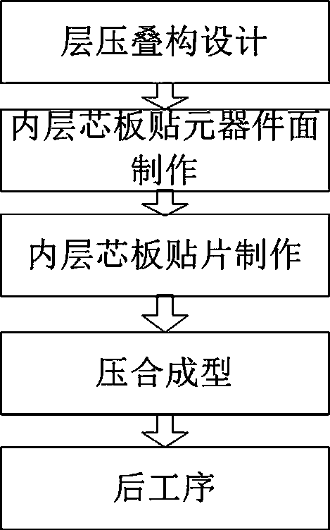
[0036] In order to enable those skilled in the art to better understand the technical solution of the present invention, the product of the present invention will be further described in detail below in conjunction with the embodiments and accompanying drawings.

[0037] Such as figure 1 As shown, the invention discloses a method for manufacturing a built-in active device PCB board, comprising the following steps:

[0038] The first step, lamination stack design, adopts a symmetrical design, avoids damage to the active device during the lamination process by controlling the thickness of the prepreg, and prevents the active device from being separated from the other by placing a prepreg without milling grooves on the top of the active device. One side is in contact with the circuit pattern, and the expansion and shrinkage compensation of the fixture is used to ensure that the expansion and contraction of each layer returns to the ratio of 1:1 after the total pressure of the inn...


PUM


Abstract

The invention discloses a manufacturing method of a PCB board internally provided with an active device. The method comprises the steps of: laminated and stacked structure designing, manufacturing of a component mounting surface of an internal core plate, internal core plate surface mounting, laminating and molding, post-processing and the like. The manufacturing method of the PCB board internally provided with the active device has the advantages that the reliability is high, the machining precision is high, the quality stability is good and the practicability is high.

Description

technical field [0001] The invention relates to the field of PCB circuit board manufacture, in particular to a method for manufacturing a PCB board with built-in active devices. Background technique [0002] At present, in order to solve the small size of the traditional PCB board, it cannot meet the increasing demand for component placement, and after the traditional PCB is placed, the components are placed outside, forming electromagnetic interference with each other, and are easily damaged by external factors. For the problem of scrapping, built-in device technology has emerged, which can effectively solve the above problems. [0003] Built-in active device PCB can well meet the development trend of light, thin and small PCB, but this technology has extremely high requirements on equipment and manufacturing process, and there are many technical difficulties. It is still in the initial test and sample processing and production stage in China. , very few manufacturers can ...

Claims


Application Information

Patent Timeline
Patent Type & Authority Patents(China)
IPC IPC(8): H05K1/18H05K3/34
CPCH05K1/186H05K3/34
Inventor 林映生林启恒武守坤陈春卫锋刘晓玲
Owner HUIZHOU KING BROTHER CIRCUIT TECH
Why Eureka
Try Eureka