Verifying method and apparatus for FPGA boundary scan system

A boundary scan and verification module technology, applied in measurement devices, instruments, measurement electronics, etc., can solve the problems of inaccurate chip measurement, the correctness of FPGA boundary scan system cannot be fully guaranteed, and achieve the effect of ensuring correctness

Active Publication Date: 2016-04-13
SHENZHEN PANGO MICROSYST CO LTD
View PDF7 Cites 3 Cited by
  • Summary
  • Abstract
  • Description
  • Claims
  • Application Information

AI Technical Summary

Problems solved by technology

[0004] Although the FPGA boundary scan system can diagnose the faults when the chip is working, the correctness of the design of the FPGA boundary scan system itself cannot be fully guaranteed, which leads to the problem of inaccurate measurement of the chip

Method used


Image

  • Verifying method and apparatus for FPGA boundary scan system
  • Verifying method and apparatus for FPGA boundary scan system
  • Verifying method and apparatus for FPGA boundary scan system

Examples


Embodiment Construction

[0060] In order to make the purpose, technical solutions and advantages of the embodiments of the present invention clearer, the technical solutions in the embodiments of the present invention will be clearly and completely described below in conjunction with the drawings in the embodiments of the present invention. Obviously, the described embodiments It is only some embodiments of the present invention, but not all embodiments. Based on the embodiments of the present invention, all other embodiments obtained by persons of ordinary skill in the art without making creative efforts belong to the protection scope of the present invention.

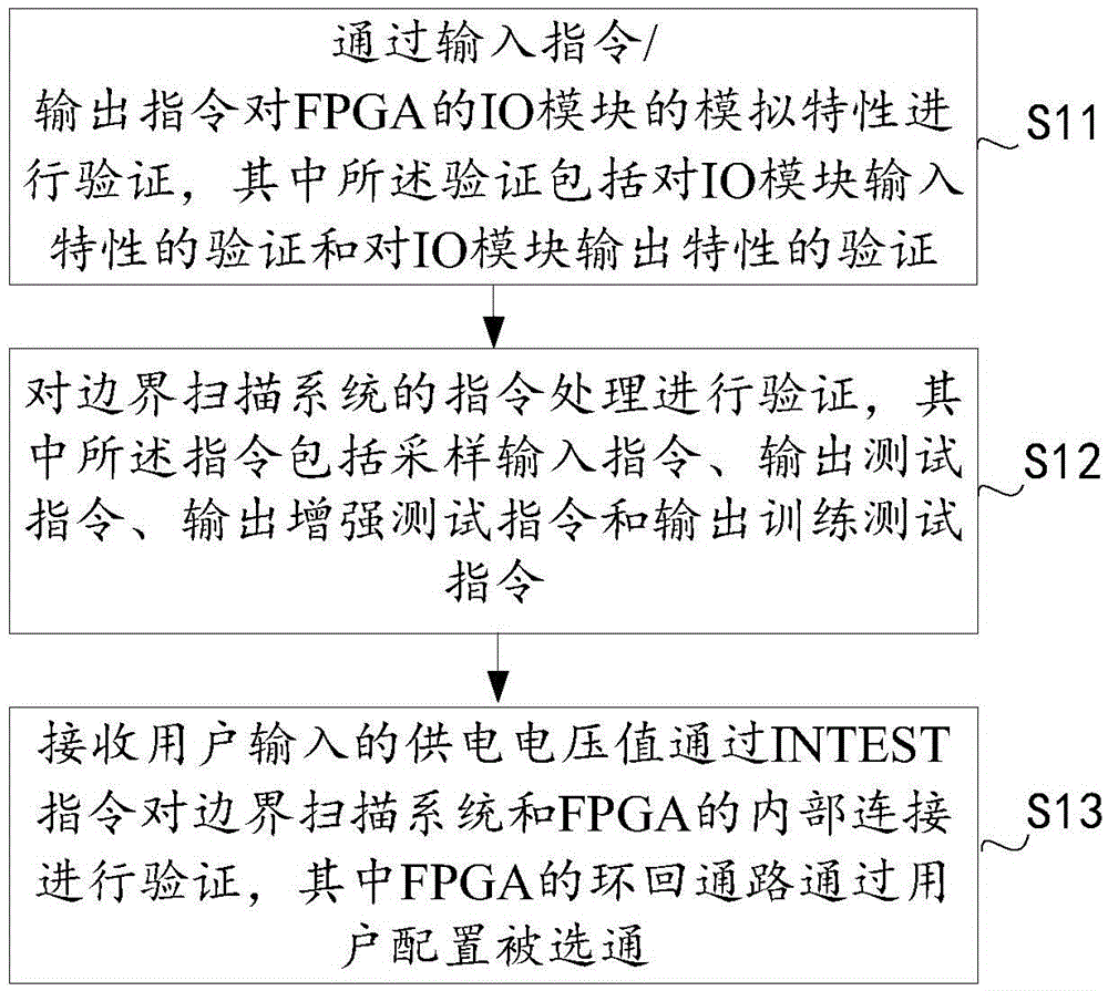
[0061] The present invention provides a kind of verification method of FPGA boundary scan system, is used for debugging FPGA boundary scan system on emulation platform, such as figure 1 As shown, the method includes:

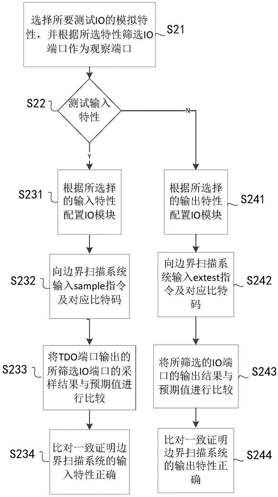
[0062] S11, verify the simulation characteristics of the input / output (IO) module of FPGA by input instruction / output instru...


PUM


Abstract

The invention provides a verifying method and apparatus for an FPGA (Field-Programmable Gate Array) boundary scan system, which are used for debugging the FPGA boundary scan system on a simulation platform. The method includes the following steps: verifying the simulation characteristics of an IO module of an FPGA through an input instruction/output instruction, wherein the verifying step includes verifying the input characteristics of the IO module and verifying the output characteristics of the IO module; verifying instruction processing of the boundary scan system, wherein instructions include a sampling input instruction, an output test instruction, an output enhancement test instruction and an output training test instruction; and verifying internal connection of the boundary scan system and the FPGA through an internal test instruction, wherein a round trip pathway of the FPGA is gated through user configuration. The verifying method and apparatus can comprehensively and thoroughly verify the FPGA boundary scan system and ensure correctness of functions of the FPGA boundary scan system.

Description

technical field [0001] The present invention relates to the technical field of ultra-large-scale programmable integrated circuits, in particular to a verification method and system for a Field-Programmable Gate Array (FPGA: Field-Programmable Gate Array) boundary scan system. Background technique [0002] With the emergence of large-scale integrated circuits, the manufacturing process of printed circuit boards has become small, micro, and thin. Traditional information and communication technology (ICT: Information Communication Technology) testing has no way to meet the testing requirements of such products. Many, the components are small in size, and the density of the board is particularly high. There is no way to perform the probe test at all, so the Joint Test Action Group (JTAG, JointTestActionGroup) boundary scan system came into being. The method of embedding the boundary scan system in the FPGA circuit design can solve the difficult problem of FPGA chip problem locat...

Claims


Application Information

Patent Timeline
Patent Type & Authority Applications(China)
IPC IPC(8): G01R35/00G01R31/3185
CPCG01R31/318597G01R35/00
Inventor 张健
Owner SHENZHEN PANGO MICROSYST CO LTD
Why Eureka
Try Eureka