A method for in-situ heat treatment of metal parts manufactured by electron beam selective melting and additive manufacturing
A technology of additive manufacturing and selective melting, which is applied in the direction of additive manufacturing, improvement of process efficiency, improvement of energy efficiency, etc., can solve the problems of increased manufacturing costs, achieve the effect of improving surface finish and eliminating microscopic holes
- Summary
- Abstract
- Description
- Claims
- Application Information
AI Technical Summary
Problems solved by technology
Method used
Image
Examples
Embodiment 1
[0026] Example 1: In-situ heat treatment of TC4 alloy
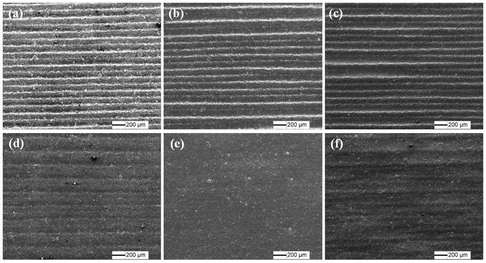
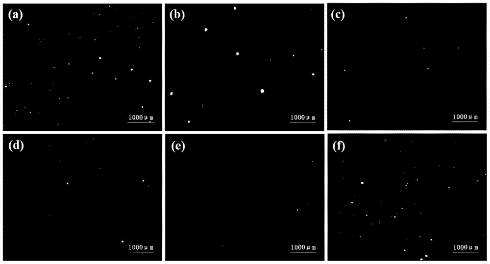
[0027] EBM equipment is used to process six TC4 alloy test blocks at the same time, and the size is 20mm×20mm×80mm. One of the test blocks was processed by the normal process, the electron beam current was 4.5mA, the scanning speed was 700m / s, the Focus Offset value was 3, and no secondary remelting in-situ heat treatment was performed. For the remaining 5 test blocks, the electron beam Focus Offset values were set to 3, 10, 20, 40, and 60 for in-situ remelting treatment, and the electron beam current and scanning speed were not changed during the remelting process. figure 2 It is the surface morphology of TC4 alloy treated with different processing parameters. from figure 2 In (a), it can be seen that there are obvious electron beam scanning traces on the surface of the unremelted sample. After the second remelting treatment, the surface state of the sample changes, and the surface of the sample obtained when the ...
Embodiment 2
[0031] Example 2: In-situ heat treatment of Inconel625 alloy
[0032] EBM equipment is used to process 4 pieces of Inconel625 alloy test blocks at the same time, and the sizes are all One of them (denoted as 1# test block) was processed by normal process, the processing electron beam current was 4.5mA, the scanning speed was 500m / s, the Focus Offset value was 20, and no secondary remelting in-situ heat treatment was performed. The parameters of the in-situ heat treatment for the other two test blocks were respectively: the electron beam current was 4.5mA, the scanning speed was 1000m / s, and the Focus Offset value was 20 (denoted as 2# test block); the electron beam current was 4.5mA, and the scanning speed was 400m / s, Focus Offset value is 40 (recorded as 3# test block). Image 6 The cross-sectional metallographic pictures and Figure 7 The electron backscatter diffraction (EBSD) images are the microscopic analysis results of the Inconel625 alloy before and after the remelt...
PUM
| Property | Measurement | Unit |
|---|---|---|
| tensile strength | aaaaa | aaaaa |
| tensile strength | aaaaa | aaaaa |
| elongation at break | aaaaa | aaaaa |
Abstract
Description
Claims
Application Information


