Voltage buffer applied to SAR (Successive Approximation Register) ADC (Analog to Digital Converter)
A voltage buffer, voltage buffer technology, applied in the direction of instruments, electrical components, adjusting electrical variables, etc., to achieve the effect of small output resistance, low static power consumption, and short settling time
- Summary
- Abstract
- Description
- Claims
- Application Information
AI Technical Summary
Problems solved by technology
Method used
Image
Examples
Embodiment Construction
[0023] The present invention will be further described below in conjunction with the accompanying drawings.
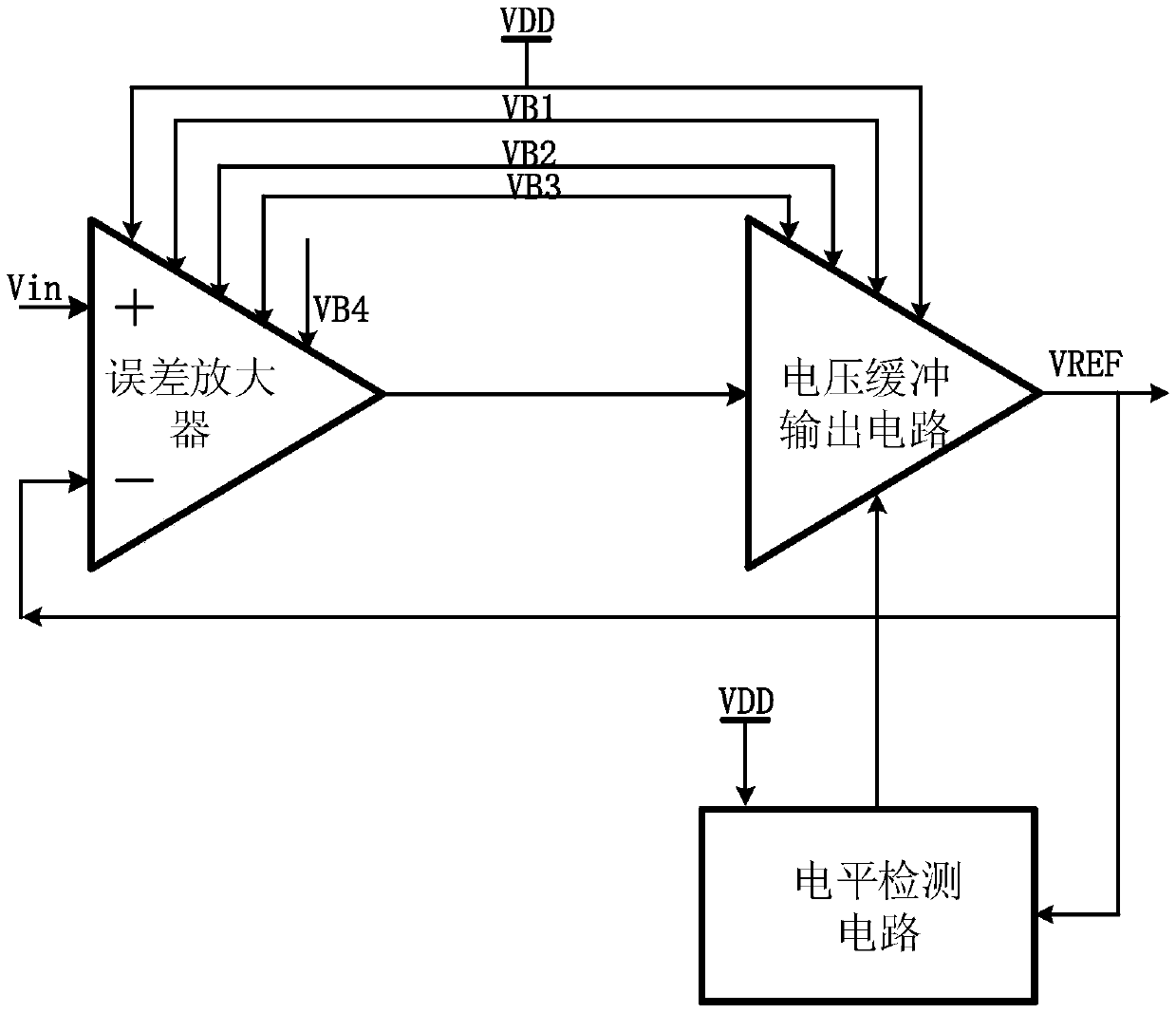
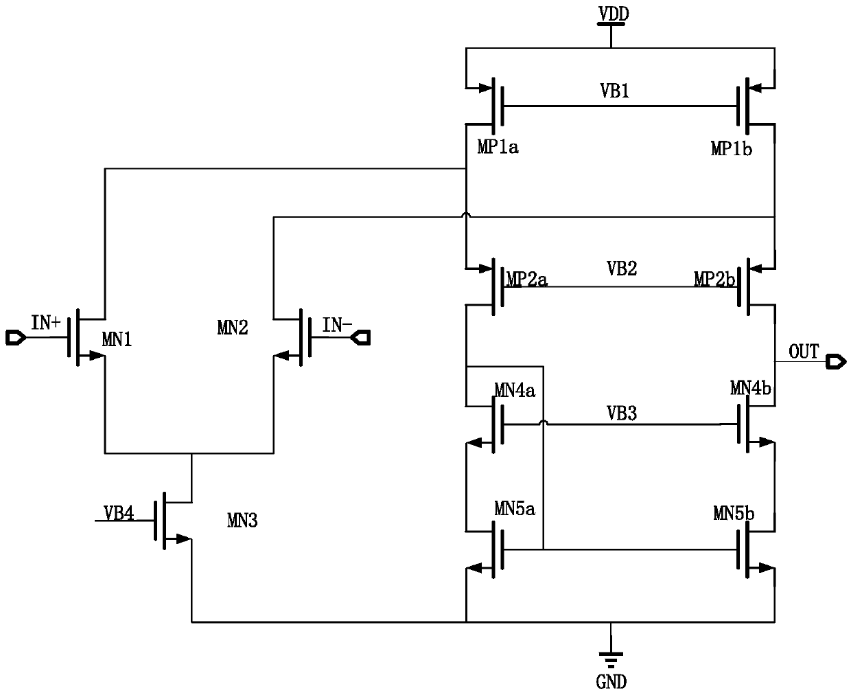
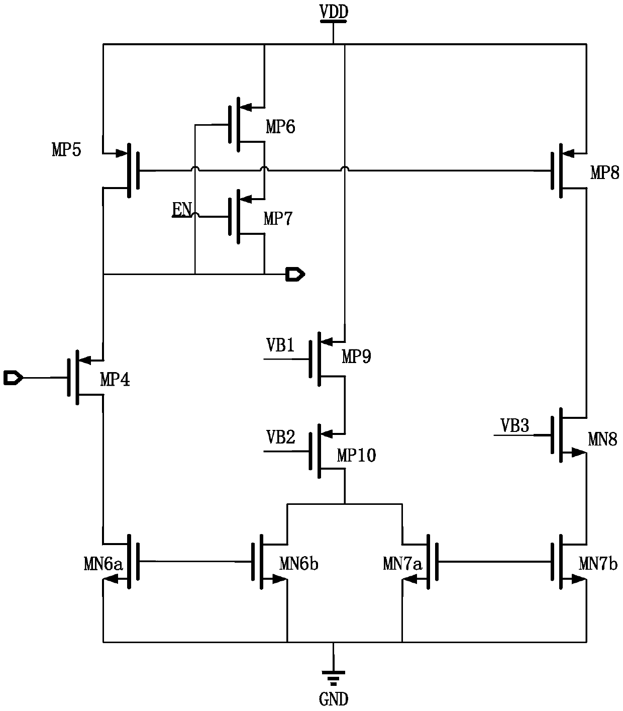
[0024] Such as figure 1 Shown is the overall block diagram of the voltage buffer applied to SARADC, including the error amplifier, voltage buffer output circuit and level detection circuit, and the DC power supply VDD supplies power to the error amplifier, voltage buffer output circuit and level detection circuit at the same time.
[0025] The first input terminal of the error amplifier is connected to the reference voltage Vin provided by the outside (bandgap reference), the second input terminal is connected to the reference voltage VREF output by the voltage buffer output circuit, the third input terminal is connected to the external bias voltage VB4, and the fourth input terminal is connected to the external bias voltage VB4. The input terminal is connected to the external bias voltage VB1, the fifth input terminal is connected to the external bias voltage VB2, and...
PUM
 Abstract
Description
Claims
Application Information


