Pixel driving chip and method and pixel structure

A technology for driving chips and pixel structures, used in instruments, semiconductor devices, electrical components, etc., can solve problems such as uncontrollable flexibility, lack of controllability, and inability to make changes

Active Publication Date: 2016-04-20
BOE TECH GRP CO LTD +1
View PDF8 Cites 28 Cited by
  • Summary
  • Abstract
  • Description
  • Claims
  • Application Information

AI Technical Summary

Problems solved by technology

In the existing driving compensation method, the threshold voltage and/or voltage drop of the driving transistor is obtained by multiplexing the display signal during the normal operation of the display device. Therefore, the existing driving compensation method is uncontrollable and relatively flexible. The disadvantages are as follows
[0007] In the normal wor...

Method used


Image

  • Pixel driving chip and method and pixel structure
  • Pixel driving chip and method and pixel structure
  • Pixel driving chip and method and pixel structure

Examples


Embodiment Construction

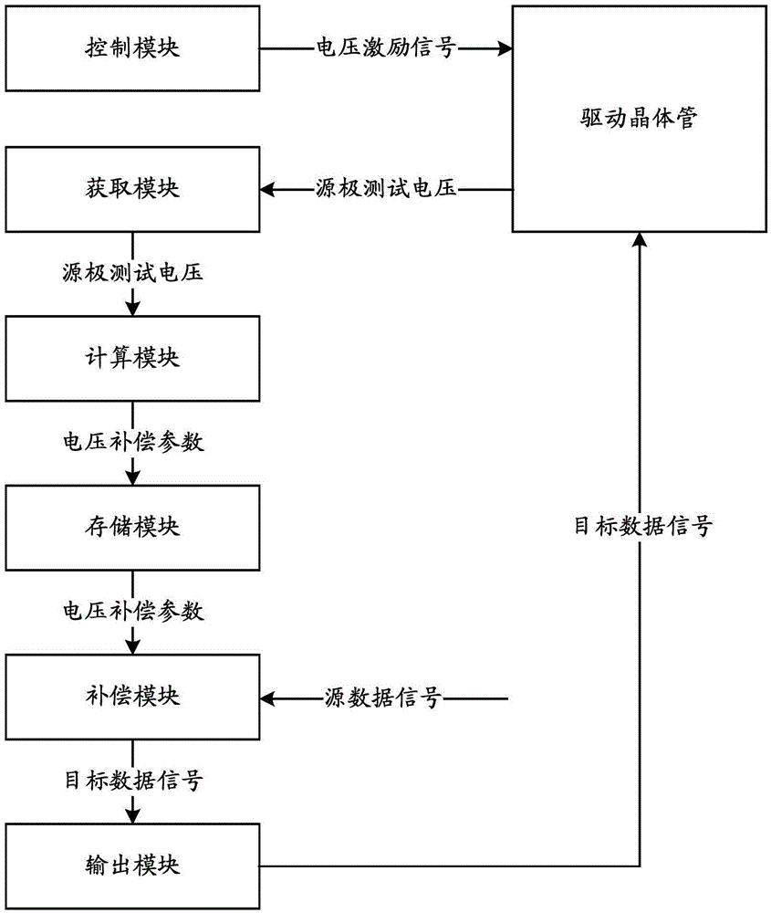
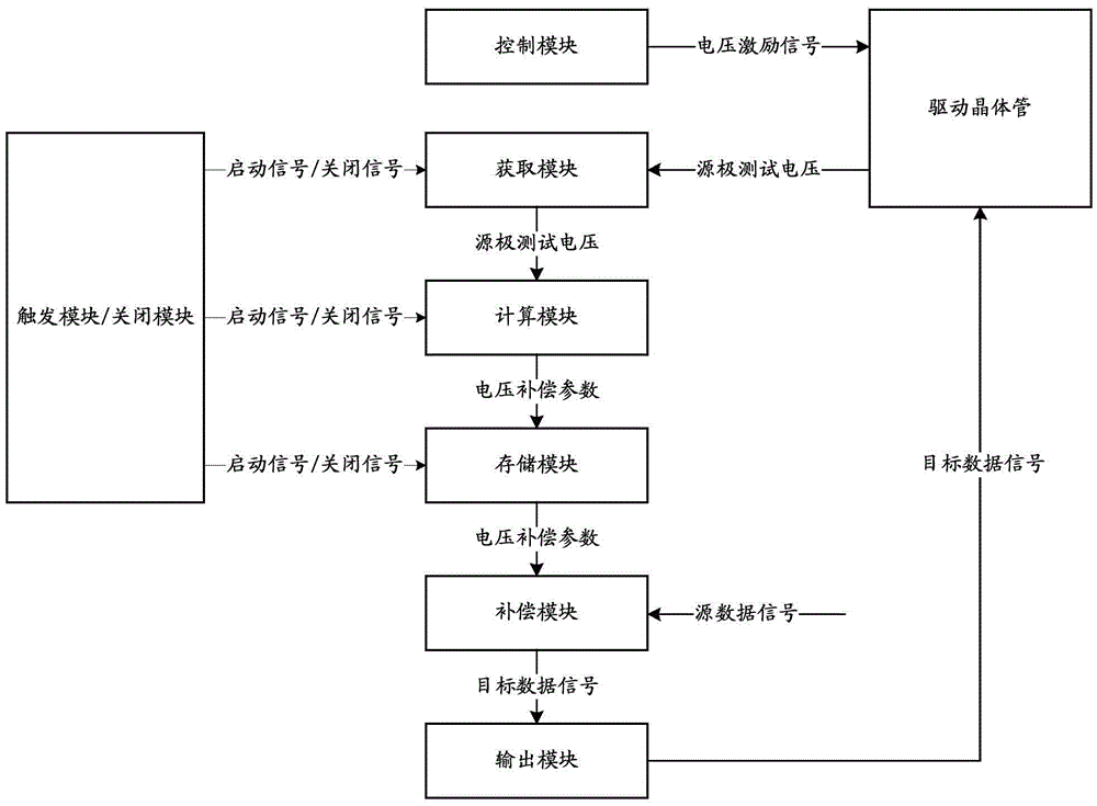
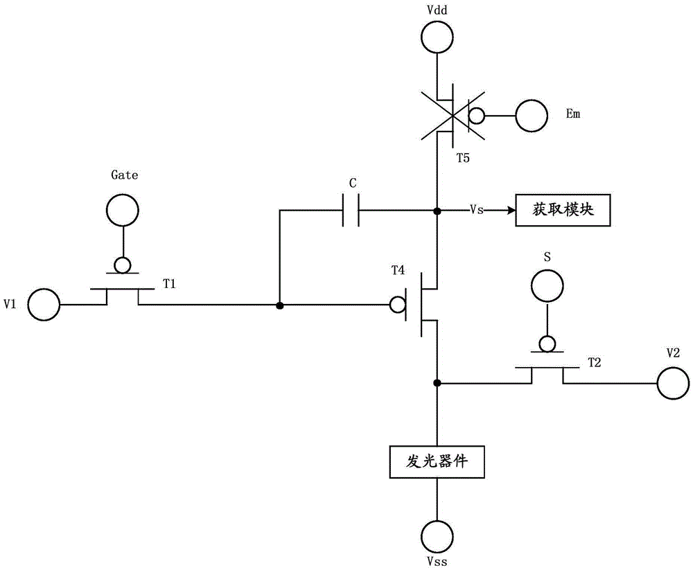
[0083] In the pixel driving chip, method, and pixel structure of the embodiments of the present invention, the pixel driving chip generates and outputs a voltage excitation signal, uses the voltage excitation signal to control the driving transistor to be in a corresponding test state, and utilizes the voltage excitation signal in the test state The source test voltage of the drive transistor is used to calculate the compensation parameters for source data signal voltage compensation. The driving transistor is controlled to be in the test state by the voltage excitation signal independent of the working signal of the pixel structure (such as data signal, switching signal, etc.), and is not affected by the normal operation of the pixel structure, thereby improving the controllability and flexibility of voltage compensation.

[0084] To achieve the above object, Embodiment 1 of the present invention provides a pixel driving chip, which is used to output target data signals to a p...


PUM


Abstract

The invention discloses a pixel driving chip and method and a pixel structure. By means of the pixel driving chip and method and the pixel structure, voltage compensation higher in controllability and better in flexibility is achieved. The pixel driving chip comprises a control module, an acquisition module, a calculation module, a storage module, a compensation module and an output module, wherein the control module is used for generating and outputting a voltage drive signal and controlling a driving transistor to be in the corresponding test state; the acquisition module is used for acquiring the source electrode test voltage of the driving transistor in the test state; the calculation module is used for calculating a voltage compensation parameter according to the source electrode test voltage, wherein the voltage compensation parameter is the voltage drop, corresponding to the power source voltage, of the threshold voltage of the driving transistor and/or a source electrode of the driving transistor; the storage module is used for storing the voltage compensation parameter; the compensation module is used for conducting voltage compensation on a source data signal by means of the stored voltage compensation parameter, so that a target data signal is obtained; the output module is used for outputting the target data signal to a grid electrode of the driving transistor. By means of the pixel driving chip and method and the pixel structure, flexibility and controllability of voltage compensation are improved.

Description

technical field [0001] The present invention relates to the technical field of pixel driving, in particular to a pixel driving chip, method and pixel structure. Background technique [0002] Organic light emitting diode (Organic Light Emitting Display, OLED) display device has many advantages such as self-illumination, low driving voltage, high luminous efficiency, short response time, high definition and contrast, near 180° viewing angle, and wide operating temperature range. The most promising display device. [0003] OLED display devices can be classified into two types, a passive matrix type and an active matrix type, according to a driving method. Wherein, the pixel structure of the active matrix OLED display device is provided with a thin film transistor (referred to as a driving transistor herein) for driving an organic light emitting diode. The threshold voltage of the driving transistor will vary with the working time, and meanwhile, the threshold voltages of diff...

Claims


Application Information

Patent Timeline
IPC IPC(8): G09G3/3225
CPCG09G3/3225G09G3/3233G09G2300/0819G09G2300/0842G09G2300/0861G09G2320/0295G09G2320/043G09G2320/045G09G2310/0256G09G3/3291G09G2300/043G09G2310/0245H10K59/123H10K59/129G09G3/325
Inventor 何小祥韦东梅祁小敬
Owner BOE TECH GRP CO LTD
Why Eureka
Try Eureka