
Ultra wideband material microwave absorber loaded with chip resistor

A technology of ultra-broadband and absorber, which is applied in the field of ultra-broadband metamaterial microwave absorber, which can solve the problems of complex preparation process, unfavorable engineering application, and limited broadening range of strong absorption band

Inactive Publication Date: 2016-04-20
WUHAN UNIV OF SCI & TECH
View PDF7 Cites 17 Cited by
  • Summary
  • Abstract
  • Description
  • Claims
  • Application Information

AI Technical Summary

Problems solved by technology

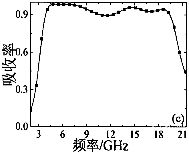
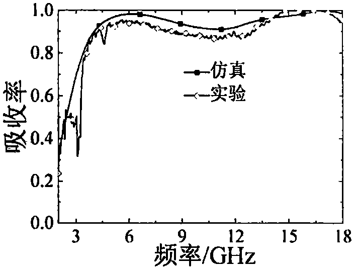
Although the proposed absorbers can broaden the microwave absorption band, the broadening range of the strong absorption band is limited (it is difficult to achieve 100% relative bandwidth if the absorption rate is greater than 90%), and the preparation process is more complicated, which is not conducive to practical engineering applications.

Method used


Image

  • Ultra wideband material microwave absorber loaded with chip resistor
  • Ultra wideband material microwave absorber loaded with chip resistor
  • Ultra wideband material microwave absorber loaded with chip resistor

Examples


Embodiment 1

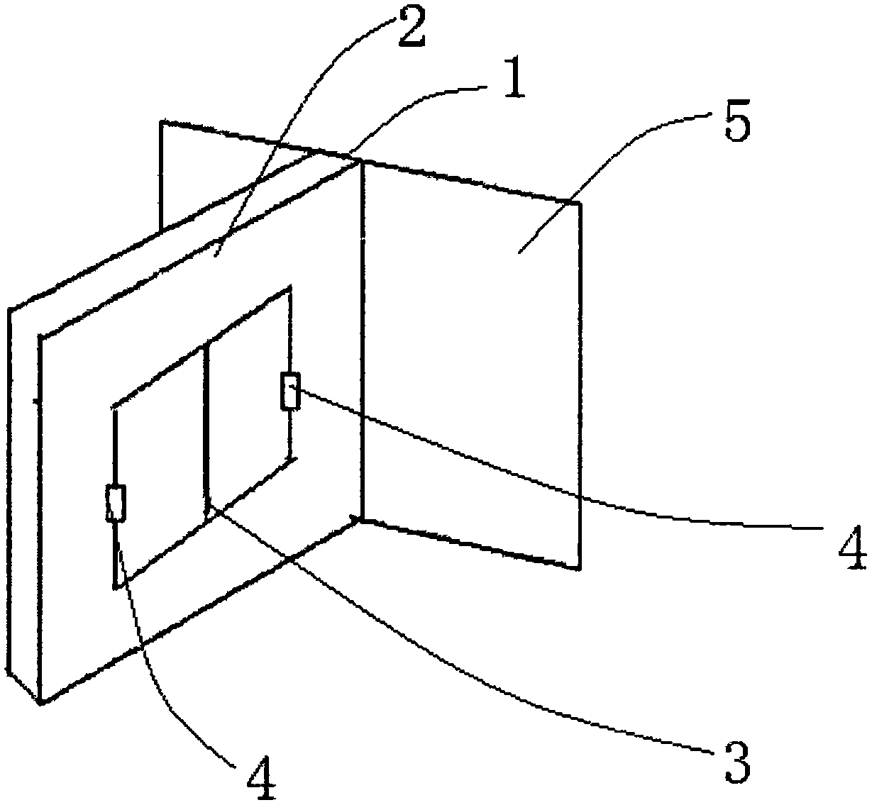
[0033] Example 1, such as figure 1 and Figure 2a and Figure 2b As shown, the absorber consists of a dielectric substrate 2, a metal slotted ring structure 3 (square metal slotted ring resonator structure) etched on the substrate, a chip resistor 4 embedded in the metal slotted ring structure 3, and a metal back Plate 5 is constructed from figure 1 The period length of the middle unit structure 1 is px and the width is py, the length of the dielectric substrate 2 is px, the width is h and the thickness is ts, the metal slotted ring structure 3 has a long side, a wide side b, a line width of w, and a slit width is g, and the resistance welded at the opening of the metal slit ring is R 1 and R 2. By changing the geometric parameters of the unit structure 1, it can work in different frequency ranges. Variation range of geometric parameters of unit structure 1:

[0034] Unit structure cycle length px width py: 5mm~50mm;

[0035] Dielectric substrate length px: 5mm~50mm; ...

Embodiment 2

[0049] Example 2, such as image 3 and Figure 4 As shown, the absorber consists of a dielectric substrate 2, a metal slotted ring structure 3 etched on the substrate (square metal double slotted ring resonator structure), a chip resistor 4 embedded in the metal slotted ring structure 3, and a metal back Plate 5 is formed, wherein, the period length of the unit structure is px and the width is py, the length of the dielectric base substrate is px, the width is h and the thickness is ts, the length of the slit ring structure is a, the broad side is b, the line width is w, and the slit width is g, the resistance welded at the opening of the slit ring is R 1 and R 2 . By changing the geometric parameters of the unit structure, it can work in different frequency ranges. The variation range of the geometric parameters of the unit structure:

[0050] Unit structure cycle length px width py: 5mm~50mm;

[0051] Dielectric substrate length px: 5mm~50mm;

[0052] Dielectric subst...

Embodiment 3

[0065] Example 3, such as Figure 5 and Figure 6 As shown, the absorber consists of a dielectric substrate 2, a metal slotted ring structure 3 etched on the substrate (circular single slotted ring resonator structure), a chip resistor 4 embedded in the metal slotted ring structure 3, and a metal The backplane is composed of 5, wherein the unit structure period length is px and the width is py, the length of the dielectric base substrate is px, the width is h and the thickness is ts, the outer ring radius of the circular slotted ring structure is r, the line width is w, and the slit width is g, the resistance welded at the opening of the slit ring is R. By changing the geometric parameters of the unit structure, it can work in different frequency ranges. The variation range of the geometric parameters of the unit structure:

[0066] Unit structure cycle length px width py: 5mm~50mm;

[0067] Dielectric substrate length px: 5mm~50mm;

[0068] Dielectric substrate width h: ...


PUM

PropertyMeasurementUnit
Thicknessaaaaaaaaaa
Thicknessaaaaaaaaaa
Thicknessaaaaaaaaaa

Abstract

The invention provides an ultra wideband material microwave absorber loaded with a chip resistor. The ultra wideband material microwave absorber comprises a unit structure and a bottom plate, wherein the unit structure is positioned on the bottom plate; the unit structure comprises a medium substrate, a metal slotting ring structure, the chip resistor and a metal back plate; the metal slotting ring structure is respectively connected with the medium substrate and the chip resistor. The ultra wideband material microwave absorber has the advantages that the strong circuit resonance and impedance matching properties are produced by the slotting ring structure loaded with the chip resistor, so that the ultra wideband impedance matching effect is realized, and the ultra wideband microwave strong absorbing effect is realized; when the electromagnetic wave is irradiated to the absorber, a magnetic field loop is generated around the resonance structure, a metal sheet and the chip resistor can produce ohm loss by the magnetic field loop, the electromagnetic energy of the electromagnetic wave is converted into heat energy by loss, then the loss of the irradiated electromagnetic wave is absorbed, and the ultra wideband high-property absorbing is realized; the structure is simple and small, the cost is low, the preparation is convenient, and the like.

Description

technical field [0001] The invention belongs to the technical field of metamaterials and electromagnetic functional materials, and relates to a microwave absorber, in particular to a polarization-insensitive ultra-wideband metamaterial microwave absorber loaded with chip resistors. Background technique [0002] Absorber, also known as wave absorber, absorber or wave-absorbing material, refers to a type of electromagnetic functional material or device that can absorb electromagnetic wave energy projected onto its surface. Microwave absorbers have also begun to play a pivotal role in many technical fields such as communication, anti-interference, environmental protection, and human body protection. Its development trend is thin thickness, strong absorption, light weight, and wide frequency band. In engineering applications, microwave absorbers are required not only to have a high absorption rate for electromagnetic waves in a wide frequency band, but also to have properties su...

Claims


Application Information

Patent Timeline
IPC IPC(8): H01Q17/00H05K9/00
CPCH01Q17/00H05K9/00
Inventor 程用志章喆周钰杰
Owner WUHAN UNIV OF SCI & TECH
Learn More