Check patentability & draft patents in minutes with Patsnap Eureka AI!

FPGA-based accelerator card and acceleration method thereof

An accelerator card and accelerator module technology, which is applied in the computer field, can solve the problems of PCI-E bus not having universality and universality, insufficient resources to solve tasks with a large amount of calculation, and limited image processing functions, so as to save processing time , low cost, simple method to achieve the effect

Active Publication Date: 2016-04-27
NO 32 RES INST OF CHINA ELECTRONICS TECH GRP
View PDF6 Cites 5 Cited by
  • Summary
  • Abstract
  • Description
  • Claims
  • Application Information

AI Technical Summary

Problems solved by technology

Using hardware acceleration such as FPGA chips to share part of the CPU work is the current mainstream solution, but there are two problems with using FPGA for hardware acceleration. One is that the resources of an FPGA accelerator are not enough to solve some complex and large-scale calculation tasks; the other is When using FPGA for co-processing and running multiple acceleration algorithms at the same time, under the same PCI-E interface, several devices coexist, and the hardware driver may be quite troublesome.
[0005] After searching, it was found that the Chinese patent application with the publication number CN102819818A provides a method for realizing image processing based on the dynamic reconfigurable technology of the FPGA chip, using the reconfigurable technology of the FPGA chip to realize the acceleration of image processing, and generating image processing Design files of the functional modules, and then configure the reconstruction module of the FPGA chip as one or more image processing functional modules for image signal processing; this method is simple to implement and low in cost, but requires pre-generated fixed image processing functions Module with limited scope of application and limited to image processing functions
The Chinese patent application with the publication number CN104657308A provides a method of server hardware acceleration implemented by FPGA, based on FPGA-based server hardware acceleration using QPI bus, by building a hardware acceleration module in the FPGA, and through the message conversion module The operation initiated by the hardware acceleration module is converted into a message and sent to the QPI bus for acceleration; this method can be configured with different acceleration algorithms to correspond to different computing applications. Although it has high flexibility and scalability, it is only applicable to the QPI bus The computer is not universal and universal to the mainstream PCI-E bus

Method used


Image

  • FPGA-based accelerator card and acceleration method thereof

Examples


Embodiment

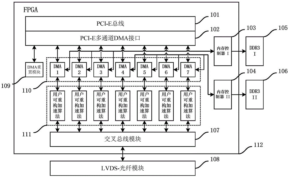
[0050] The present embodiment provides a kind of acceleration method based on FPGA accelerator card, comprises following process:

[0051] Build PCI-E bus interface module, multiple DMA, DMA reset module, multiple user reconfigurable acceleration modules, LVDS-fiber module, cross bus module and DDR3 control module inside FPGA.

[0052] The specific method is:

[0053] A PCI-E bus interface module is built inside the FPGA, and the PCI-E bus interface module includes a PCI-E bus and a PCI-E multi-channel DMA interface. The outside of the PCI-E bus interface module is connected to the PC through the PCI-E bus, and the inside of the PCI-E bus interface module uses a unified PCI-E multi-channel DMA interface to connect with multiple DMAs. It mainly supports read and write access to the memory controller by other DMAs inside the FPGA, and supports byte misalignment.

[0054] Multiple DMAs are constructed inside the FPGA, and the DMAs are connected to the PCI-E bus interface module...


PUM


Abstract

The present invention provides an acceleration method of an FPGA-based accelerator card. The acceleration method comprises the following process of constructing a PCI-E bus interface module, a plurality of DMAs, a DMA reset module, a plurality of user-reconfigurable acceleration modules, an LVDS-optical fiber module, a crossed bus module and DDR3 control modules in an FPGA. The present invention also provides an accelerator card obtained by utilization of the acceleration method. The FPGA-based accelerator card and the acceleration method thereof are simple in implementation method and low in cost; the plurality of DMAs and the plurality of user-reconfigurable acceleration modules are configured, processing time is saved by decomposing the task and performing parallel computing, and processing efficiency is improved; a plurality of accelerator cards can be crossed through LVDS and optical fiber and can be freely expanded according to application requirements; and by utilization of the reconfigurable characteristics of the FPGA, different acceleration applications can be achieved by loading different bit steam files, and application range is wide.

Description

technical field [0001] The invention relates to the technical field of computers, in particular to an FPGA-based acceleration card and an acceleration method thereof. Background technique [0002] FPGA (Field-Programmable Gate Array), that is, field programmable gate array, is the product of the development of programmable devices such as PAL, GAL, and CPLD. The device was first launched by Xilinx in 1985. It is a new type of high-density PLD, which is made by CMOS-SRAM technology. The structure of FPGA is divided into three parts: programmable logic module, programmable I / O module and programmable internal interconnection area IR. There are many programmable logic units (LE, LogicElement) inside the FPGA. Users can program these programmable modules on-site to achieve different logic functions. Compared with application-specific integrated circuits, FPAG has higher flexibility and development The cycle is shorter and the single integration is lower. FPGA can be programme...

Claims


Application Information

Patent Timeline
Patent Type & Authority Applications(China)
IPC IPC(8): G06F13/38G06F13/40G06F13/28
CPCG06F13/28G06F13/385G06F13/4022G06F2213/0008G06F2213/0024
Inventor 陈静马克杰俞则人
Owner NO 32 RES INST OF CHINA ELECTRONICS TECH GRP
Features
  • R&D
  • Intellectual Property
  • Life Sciences
  • Materials
  • Tech Scout
  • Unparalleled Data Quality
  • Higher Quality Content
  • 60% Fewer Hallucinations
Learn More