Test method for ion implantation machine base

An ion implanter and ion implantation technology, applied in semiconductor/solid-state device testing/measurement, electrical components, circuits, etc., to achieve simple operation, accurate results, and stable thickness

Active Publication Date: 2016-05-04
SHANGHAI HUAHONG GRACE SEMICON MFG CORP
View PDF4 Cites 5 Cited by
  • Summary
  • Abstract
  • Description
  • Claims
  • Application Information

AI Technical Summary

Problems solved by technology

[0004] However, there is currently no effective method to monitor the effect of ion implantation on the subsequent growth of oxide layer thickness on the polysilicon surface

Method used


Image

  • Test method for ion implantation machine base
  • Test method for ion implantation machine base
  • Test method for ion implantation machine base

Examples


Embodiment Construction

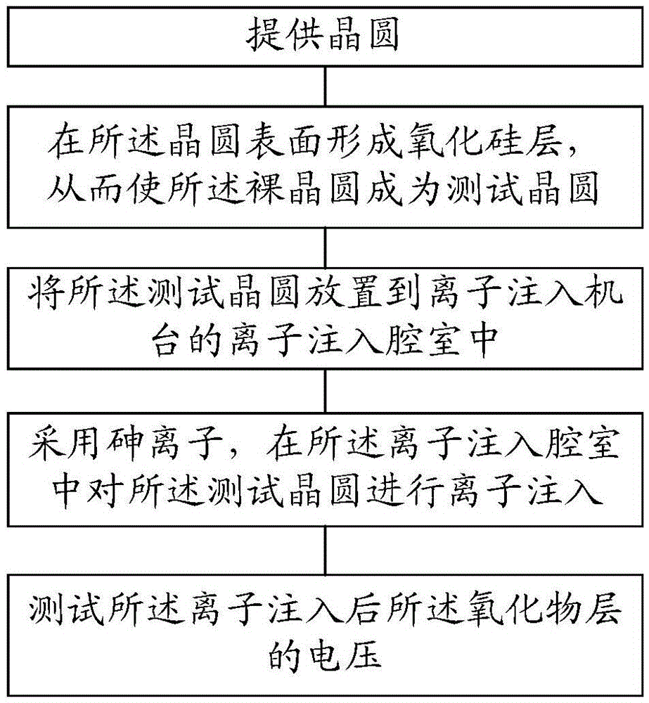
[0028] For the equipment of the ion implantation process, the abnormal conditions of the equipment will affect the growth effect of the oxide layer on the polysilicon surface. If the corresponding product is produced in a poor condition of the chamber of the machine, it will affect the growth of the subsequent oxide layer and affect the electrical characteristics of the final device. Therefore, it is very important to monitor the condition of the chamber during the ion implantation process. However, there is currently no effective method to monitor the effect of ion implantation on the thickness of the subsequently grown oxide layer on the polysilicon surface.

[0029] For this reason, the present invention provides a new test method for ion implantation equipment to directly monitor the growth and production status of the oxide layer of polysilicon after ion implantation.

[0030] In order to make the above objects, features and advantages of the present invention more compre...


PUM


Abstract

The invention discloses a test method for an ion implantation machine base. The test method is used for testing whether the ion implantation machine base is suitable for ion implantation for polycrystalline silicon or not so as to ensure stable thickness of an oxide layer growing on the surface of the polycrystalline silicon in a subsequent thermal oxidization process. The test method comprises the steps of providing a wafer; forming the oxide layer on the surface of the wafer so as to enable the wafer to be a tested wafer; putting the tested wafer into an ion implantation cavity of the ion implantation machine base; performing ion implantation for the tested wafer in the ion implantation cavity; and after performing ion implantation, measuring charges of the oxide layer, and judging whether the ion implantation machine base is suitable for ion implantation for polycrystalline silicon or not according to the charges. According to the test method, whether the ion implantation machine base is suitable for ion implantation for polycrystalline silicon or not can be accurately judged so as to ensure stable thickness of the oxide layer growing on the surface of the polycrystalline silicon in the subsequent thermal oxidization process.

Description

technical field [0001] The invention relates to the field of semiconductor manufacturing, in particular to a test method for an ion implantation machine. Background technique [0002] With the development of semiconductor technology, more and more semiconductor products need to control the growth thickness of the oxide layer by implanting impurities on the polysilicon film, so as to prevent the polysilicon that needs to be retained from being removed in the subsequent grinding and etching process. . [0003] Traditionally, the method of monitoring the growth thickness of the oxide layer of polysilicon after ion implantation is through the method of resistance value testing. That is, the ion-implanted wafer is used for high-temperature thermal annealing, and then the state of ion implantation under the existing cavity condition is obtained according to the wafer. However, this method is only applicable to the subsequent process of growing wafers without an oxide layer. Mor...

Claims


Application Information

Patent Timeline
Patent Type & Authority Applications(China)
IPC IPC(8): H01L21/66
CPCH01L22/30
Inventor 姚雷张凌越朱云国子明范世炜郭国超
Owner SHANGHAI HUAHONG GRACE SEMICON MFG CORP
Why Eureka
Try Eureka