Diode assist-triggered thyristor device and manufacturing method and integrated circuit thereof
A diode-assisted and manufacturing method technology, applied in semiconductor/solid-state device manufacturing, circuits, semiconductor devices, etc., can solve problems such as increased design costs, protection devices that cannot be turned on in time, and long device turn-on time
- Summary
- Abstract
- Description
- Claims
- Application Information
AI Technical Summary
Problems solved by technology
Method used
Image

Examples
Embodiment 1
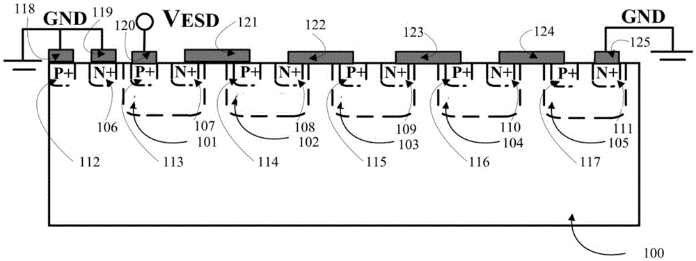
[0036] figure 1 It is a structural schematic diagram of a DTSCR device in the prior art, figure 1 Including five N well regions, specifically: P-type substrate 100;
[0037] On the P-type substrate 100, a first P+ implant region 112, a first N+ implant region 106, N well regions 101, 102, 103, 104 and 105 are sequentially formed, and a second P+ implant region and a second P+ implant region are formed in each N well region. The second N+ implant region, as shown in the figure, forms the second P+ implant region 113 on the side close to the first P+ implant region in the N well region 101, and forms the second N+ implant region 107 on the side away from the first P+ implant region ; In the N well region 102, a second P+ implant region 114 is formed on the side close to the first P+ implant region, and a second N+ implant region 108 is formed on the side away from the first P+ implant region; in the N well region 103, it is close to the first One side of the P+ implantation re...
Embodiment 2
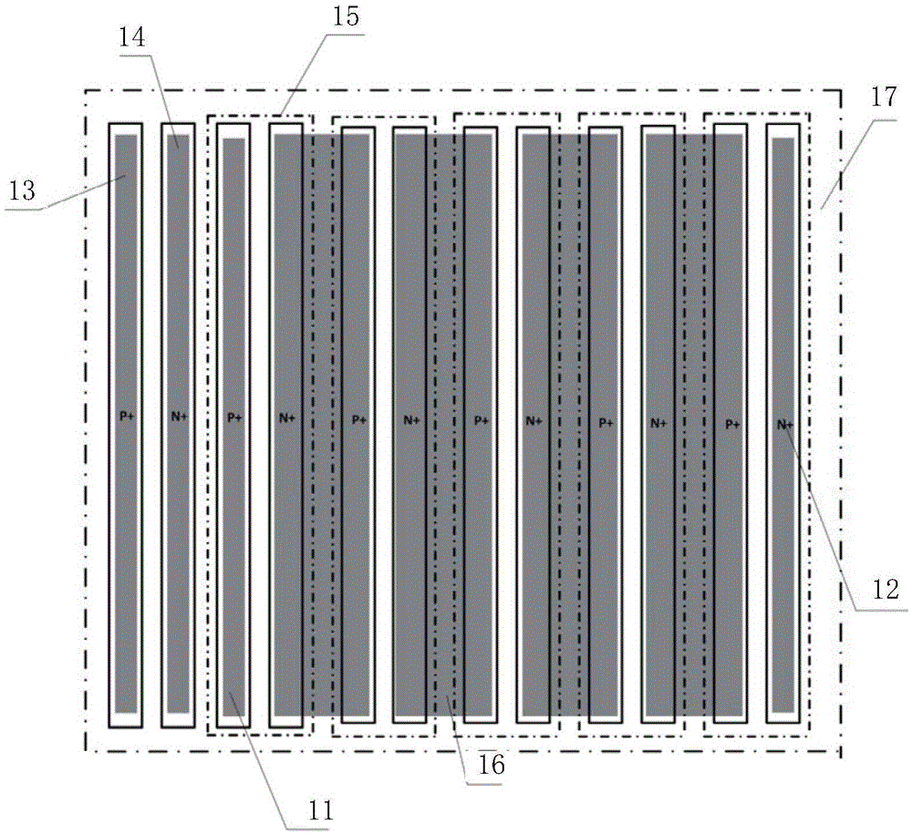
[0056] On the basis of Embodiment 1, in the diode-assisted triggering thyristor device provided in this embodiment, the area of the pattern formed on the surface of the substrate by the second P+ implantation region and the second N+ implantation region is along the direction away from the first P+ implantation region direction decreases and the areas of the second P+ implantation region and the second N+ implantation region located in the same N well region are equal.
[0057] It should be noted that the area of the pattern formed by the second P+ implantation region and the second N+ implantation region on the surface of the substrate decreases along the direction away from the first P+ implantation region. This design method ensures that the current gradually increases. , to avoid the damage of the device caused by the accumulation of current in the area of sudden change of area.
[0058] On the other hand, when the areas of the second P+ implantation region and the s...
Embodiment 3
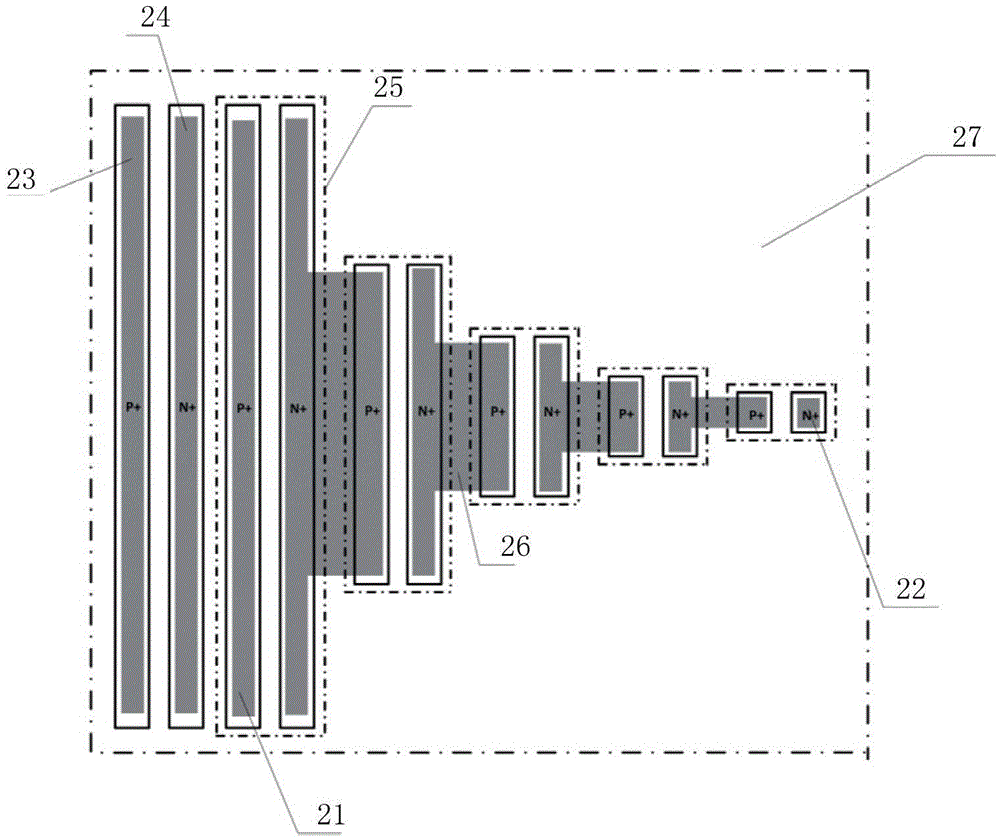
[0061] On the basis of Embodiment 1, the diode-assisted triggering thyristor device provided in this embodiment includes a first P+ injection region, a first N+ injection region, a second P+ injection region closest to the first P+ injection region, and The pattern formed on the surface of the P-type substrate by the second N+ implanted region closest to the first P+ implanted region is a rectangle with equal areas and equal long sides, and the lines connecting the center points of all the rectangles are perpendicular to the long side.
[0062] Ensure that the injection region used for charge release on the substrate has the same area as the injection region in the well region closest to the injection region, which increases the interaction between the injection region in the well region and the injection region outside the well region The region area ensures the release effect of the first P+ implantation region and the first N+ implantation region.
[0063] The thyristor de...
PUM
 Abstract
Description
Claims
Application Information
 - R&D
- Intellectual Property
- Life Sciences
- Materials
- Tech Scout
- Unparalleled Data Quality
- Higher Quality Content
- 60% Fewer Hallucinations
Browse by: Latest US Patents, China's latest patents, Technical Efficacy Thesaurus, Application Domain, Technology Topic, Popular Technical Reports.
© 2025 PatSnap. All rights reserved.Legal|Privacy policy|Modern Slavery Act Transparency Statement|Sitemap|About US| Contact US: help@patsnap.com