Microstructure enhanced absorption photosensitive devices

A microstructured, enhanced technology that can be used in optics, light guides, optical components, etc., to solve problems such as high multiplication noise and high cost

Active Publication Date: 2016-05-04
王士原 +1
View PDF2 Cites 54 Cited by
  • Summary
  • Abstract
  • Description
  • Claims
  • Application Information

AI Technical Summary

Problems solved by technology

However, both InGaAs devices and Ge devices are relatively expensiv

Method used


Image

  • Microstructure enhanced absorption photosensitive devices
  • Microstructure enhanced absorption photosensitive devices
  • Microstructure enhanced absorption photosensitive devices

Examples


Embodiment Construction

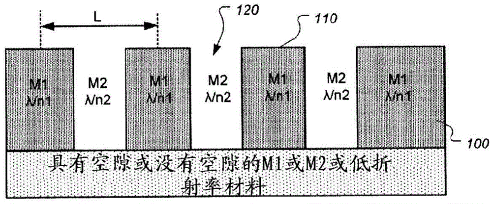
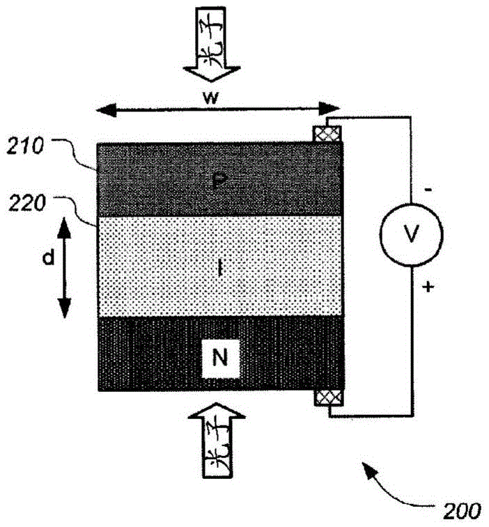
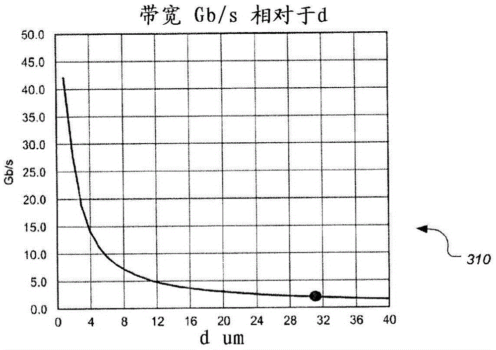
[0077]A detailed description of examples of preferred embodiments is provided below. While several embodiments have been described, it should be understood that the novel subject matter described in this patent specification is not limited to any one or combination of embodiments described herein, but encompasses numerous alternatives, modifications, and equivalent program. In addition, although numerous specific details are set forth in the following description in order to provide a thorough understanding, some embodiments may be practiced without some or all of these details. Also, for the purpose of clarity, certain technical material that is known in the related art has not been described in detail to avoid unnecessarily obscuring new subject matter described herein. It should be clear that individual features of one or several of the specific embodiments described herein may be used in combination with features or other described embodiments. In addition, the same refe...


PUM


Abstract

Techniques for enhancing the absorption of photons in semiconductors with the use of microstructures are described. The microstructures, such as pillars and/or holes, effectively increase the effective absorption length resulting in a greater absorption of the photons. Using microstructures for absorption enhancement for silicon photodiodes and silicon avalanche photodiodes can result in bandwidths in excess of 10 Gb/s at photons with wavelengths of 850 nm, and with quantum efficiencies of approximately 90% or more.

Description

[0001] References to related applications [0002] This patent application claims priority to each of the following applications, and each of the following applications is incorporated herein by reference: [0003] U.S. Provisional Application No. 61 / 826,446, filed May 22, 2013; [0004] U.S. Provisional Application No. 61 / 834,873, filed June 13, 2013; [0005] U.S. Provisional Application No. 61 / 843,021, filed July 4, 2013; and [0006] U.S. Provisional Application No. 61 / 905,109, filed November 15, 2013; [0007] The provisional patent applications referenced above are collectively referred to herein as the "commonly assigned, incorporated applications." technical field [0008] The present invention generally relates primarily to photosensitive devices. More specifically, some embodiments relate to photosensitive devices having microstructure-enhanced absorption properties. Background technique [0009] Fiber optic communications are widely used in applications such ...

Claims


Application Information

Patent Timeline
IPC IPC(8): H01L31/02H01L31/0352H01L31/07
CPCH01L31/035227Y02E10/52Y02E10/548H01L31/075H01L31/035272H01L31/1075Y02E10/544Y02E10/547H01L31/035281H01L31/107H01L31/028H01L31/02161H01L31/105H01L31/022408H01L31/022466G02B6/136G02B2006/12176H01L31/0284H01L31/022475H01L31/035209H01L31/0312H01L31/036H01L31/077H01L31/1808H01L31/1812H01L31/1055H01L31/054G02B6/122G02B2006/12097H01L23/66H01L31/02005H01L31/02019H01L31/02327H01L31/02363H01L31/024H01L31/0304H01L31/03046H01L31/0745H01L31/1804H01L31/184H01L31/1844H01L2223/6627
Inventor 王士原王士平
Owner 王士原
Why Eureka
Try Eureka