Fan-out type 3D packaging structure embedded in silicon substrate

A packaging structure and silicon substrate technology, applied in semiconductor/solid-state device components, semiconductor devices, electrical components, etc., can solve problems such as thermal expansion coefficient mismatch, achieve good reliability, achieve miniaturization, and easy miniaturization effects

Active Publication Date: 2016-05-11
HUATIAN TECH KUNSHAN ELECTRONICS
View PDF9 Cites 44 Cited by
  • Summary
  • Abstract
  • Description
  • Claims
  • Application Information

AI Technical Summary

Problems solved by technology

[0011] In order to solve the above technical problems, the present invention proposes a fan-out 3D packaging structure embedded in a silicon substrate, using a silicon substrate instead of molding compound or other non-silicon materials as the fan-out matrix, which solves the problems caused by the reconstruction of the wafer ...

Method used


Image

  • Fan-out type 3D packaging structure embedded in silicon substrate
  • Fan-out type 3D packaging structure embedded in silicon substrate
  • Fan-out type 3D packaging structure embedded in silicon substrate

Examples


Embodiment Construction

[0037] In order to understand the technical content of the present invention more clearly, the following examples are given in detail, the purpose of which is only to better understand the content of the present invention but not to limit the protection scope of the present invention. The components in the structures in the drawings of the embodiments are not scaled according to the normal scale, so they do not represent the actual relative sizes of the structures in the embodiments.

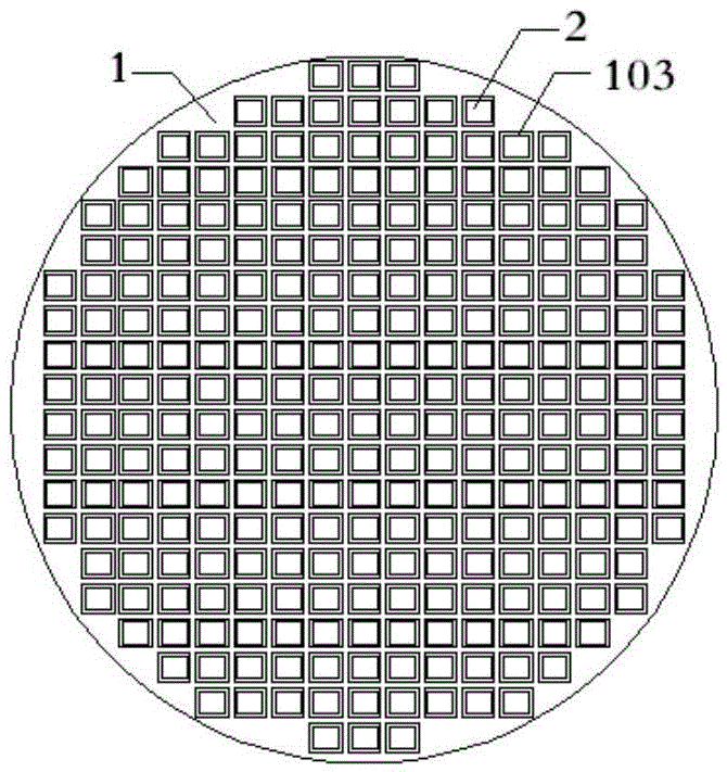
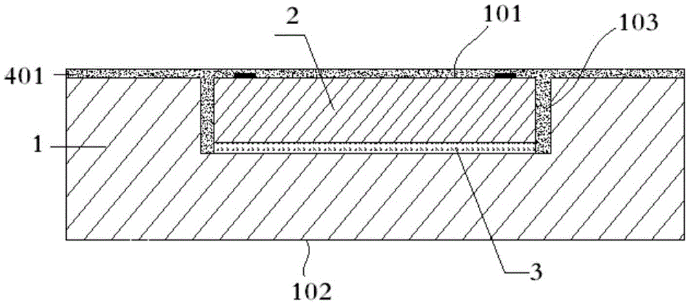
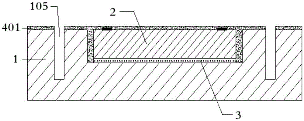
[0038] Such as Figure 11As shown, a fan-out 3D packaging structure embedded in a silicon substrate includes a silicon substrate 1 and at least one functional chip 2 . The silicon substrate 1 encloses other surfaces of the functional chip without the functional surface through the groove 103. There is an adhesive layer between the functional chip 2 and the silicon substrate 1, and there are several vertical conductive through holes 104 near the groove on the silicon substrate 1. At least one pa...


PUM


Abstract

The invention discloses a fan-out type 3D packaging structure embedded in a silicon substrate. In the packaging structure, a functional chip is embedded into a groove formed in the front surface of the silicon substrate; vertical conductive through holes are formed in a region outside the groove formed in the front surface of the silicon substrate; the functional chip can be used for conducting electricity to the back surface of the silicon substrate; and a rearrangement wire and a welding ball are arranged on the front surface and back surface of the silicon substrate. The structure has the advantages that the thermal expansion coefficients of the silicon substrate and the chip are close so that the packaging structure has good reliability; the structure can realize 3D packaging interconnection; the silicon substrate is adopted, a thin-line and high-density rearrangement wire can be produced, and the requirements on high-density interconnection can be met; and the packaging structure can relatively easily realize miniaturization and thinness, a preparation method is developed and a process is feasible.

Description

technical field [0001] The invention relates to the technical field of electronic packaging, in particular to a fan-out 3D packaging structure embedded in a silicon substrate. Background technique [0002] In the current semiconductor industry, electronic packaging has become an important direction of industry development. The development of packaging technology for decades has made high-density, small-size packaging requirements become the mainstream direction of packaging. [0003] Wafer-level fan-out packaging, by reconstructing the wafer and wafer-level rewiring method, the I / O is covered with the rewiring area array on the package surface, so as to expand the I / O pitch and meet the next level of interconnection pitch requirements. At present, the materials for reconstituting wafers are mainly molding compounds, or organic materials such as prepregs for substrate packaging, to realize the plastic packaging of functional chip fan-out structures, and finally cut into sing...

Claims


Application Information

Patent Timeline
IPC IPC(8): H01L23/06H01L23/48H01L23/485H01L21/60
CPCH01L23/06H01L23/481H01L24/16H01L24/24H01L24/91H01L2224/02379H01L2224/16H01L2224/2413H01L24/19H01L24/29H01L24/32H01L24/73H01L24/82H01L24/92H01L24/97H01L2224/04105H01L2224/12105H01L2224/24227H01L2224/2919H01L2224/32225H01L2224/73267H01L2224/82039H01L2224/92244H01L2224/97H01L2924/15153H01L2924/15311H01L2924/157H01L2924/3511H01L2224/82031H01L2224/83H01L23/485H01L23/528H01L21/4853H01L21/486H01L23/13H01L23/147H01L23/3192H01L23/49816H01L23/49827H01L23/49838H01L23/5389H01L2224/0231H01L2224/13024H01L2924/0665
Inventor 于大全
Owner HUATIAN TECH KUNSHAN ELECTRONICS
Why Eureka
Try Eureka