High-density PCB high-efficiently suppressing edge radiation and method for suppressing edge radiation

A technology of PCB board and edge radiation, which is applied in the field of high-density PCB board and edge radiation suppression efficiently suppressing edge radiation, can solve the problems of unsatisfactory suppression effect and connection method affecting EMI effect, etc., so as to improve signal integrity performance, improve Power transfer performance, power reduction effect

Active Publication Date: 2016-05-18
SYSU CMU SHUNDE INT JOINT RES INST +1
View PDF3 Cites 3 Cited by
  • Summary
  • Abstract
  • Description
  • Claims
  • Application Information

AI Technical Summary

Problems solved by technology

The 20-H guideline is just a rule of thumb, and the suppression achieved in many cases is not ideal
Embedded planar capacitors need to use short-circuit holes to connect noise to the entire current loop of the PCB, so the connection method of the short-circuit holes also affects the effect of EMI

Method used


Image

  • High-density PCB high-efficiently suppressing edge radiation and method for suppressing edge radiation
  • High-density PCB high-efficiently suppressing edge radiation and method for suppressing edge radiation
  • High-density PCB high-efficiently suppressing edge radiation and method for suppressing edge radiation

Examples


Embodiment 1

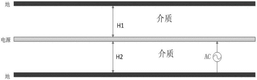
[0036] 1. Experimental board prototype selection of the present invention.

[0037] The present invention takes the three-layer PCB board with the most common size as the experimental board prototype, the size is 80mm×120mm, the dielectric material is the most commonly used FR4 with a dielectric constant of 4.4, the thickness of the dielectric layer is 0.4mm, and the power supply / The thickness of the ground plane layer is 0.03mm. The excitation source is the lumped port excitation, which is located on the lower right side of the PCB, such as figure 1 shown.

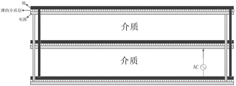
[0038] 2. Embedded planar capacitor stack design that suppresses edge radiation.

[0039] For such prototyping boards, electromagnetic radiation is generated for various reasons. The current path is interrupted at the edge of the plane, the impedance changes suddenly, the signal is emitted and rings, and the spectrum peaks at the ringing frequency, which intensifies the radiation. The power / ground plane pair constitu...


PUM


Abstract

The invention relates to a high-density PCB high-efficiently suppressing edge radiation and a method for suppressing edge radiation. The EMI of the PCB mainly derives from a power distribution network. A power / ground plane in the power distribution network forms a resonant cavity which may cause serious electromagnetic radiation at resonant frequency. The high-density PCB and the method for suppressing edge radiation may high-efficiently shield the electromagnetic radiation in the power / ground and reduce the EMI to an ideal state. A laminate is an embedded planar capacitor laminate. The embedded planar capacitor formed by a thin dielectric and power ground plane pair can be viewed as AC short circuit at a high frequency band and may achieve a very good electromagnetic radiation suppression effect.

Description

technical field [0001] The invention relates to the field of PCB boards, and more particularly to a high-density PCB board and an edge radiation suppression method for efficiently suppressing edge radiation. Background technique [0002] With the rapid development of semiconductor technology, the integration scale of electronic systems is getting bigger and bigger, the volume is getting smaller, the speed is getting faster, and the functions are getting more powerful. But it is precisely because many transistors are integrated into a single chip, the power consumption of processors and chips continues to increase, the supply voltage continues to decrease, the voltage noise margin also decreases, electromagnetic radiation continues to increase, and signal integrity problems It's getting tougher. The problem of electromagnetic interference (EMI) has become a huge challenge for the design of high-speed digital systems. [0003] PCB edge radiation suppression is a part of high...

Claims


Application Information

Patent Timeline
Patent Type & Authority Applications(China)
IPC IPC(8): H05K1/02
CPCH05K1/0216H05K2201/093
Inventor 张木水邓春业
Owner SYSU CMU SHUNDE INT JOINT RES INST
Why Eureka
Try Eureka