Anti-static device as well as production method and substrate thereof

一种防静电、器件的技术,应用在半导体/固态器件制造、电固体器件、电气元件等方向,能够解决像素电路受损、过孔03长度大、难以制作等问题,达到降低电断开的概率、减小长度、防止静电击穿的效果

Active Publication Date: 2016-05-25
BOE TECH GRP CO LTD +1
View PDF9 Cites 9 Cited by
  • Summary
  • Abstract
  • Description
  • Claims
  • Application Information

AI Technical Summary

Problems solved by technology

Electrostatic breakdown will cause damage to the pixel circuit on the array substrate in the display device, and in severe cases, it will cause a short circuit on the pixel circuit on the array substrate, and the array substrate will not work normally
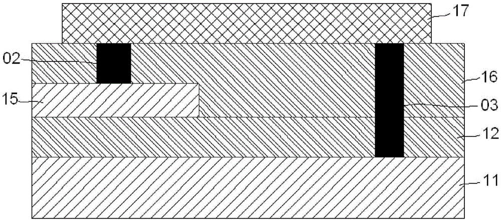
[0006] In addition, if figure 1 As shown, in the prior art, the via hole 03 electrically connecting the third conductive layer 17 and the first conductive layer 11 needs to penetrate through the first insulating layer 12 and the second insulating layer 13, which results in a relatively large length of the via hole 03, Difficult to make
Sometimes the actually formed via hole 03 cannot completely penetrate the first insulating layer 12 and the second insulating layer 16, which will cause the third conductive layer 17 to be unable to be electrically connected to the first conductive layer 11, increasing the connection between the third conductive layer 17 and the first insulating layer 16. Probability of electrical disconnection (OPEN) between conductive layers 11

Method used


Image

  • Anti-static device as well as production method and substrate thereof
  • Anti-static device as well as production method and substrate thereof
  • Anti-static device as well as production method and substrate thereof

Examples


Embodiment Construction

[0028] The technical solutions of the present invention will be further specifically described below through the embodiments and in conjunction with the accompanying drawings. In the specification, the same or similar reference numerals designate the same or similar components. The following description of the embodiments of the present invention with reference to the accompanying drawings is intended to explain the general inventive concept of the present invention, but should not be construed as a limitation of the present invention.

[0029] In addition, in the following detailed description, for purposes of explanation, numerous specific details are set forth in order to provide a comprehensive understanding of the embodiments of the present disclosure. It may be evident, however, that one or more embodiments may be practiced without these specific details. In other instances, well-known structures and devices are shown in diagrammatic form to simplify the drawings.

[0...


PUM


Abstract

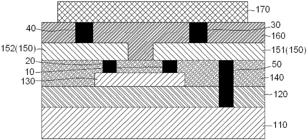
The invention discloses an anti-static device as well as a production method and a substrate thereof. The anti-static device comprises a first conducting layer, a first insulating layer, an active layer, an etch-resisting layer, and a second conducting layer, wherein the first insulating layer is formed on the first conducting layer; the active layer is formed on the first insulating layer; the etch-resisting layer is formed on the active layer; the second conducting layer is formed on the etch-resisting layer, and comprises a first part and a second part which are spaced from each other; the first part and the second part of the second conducting layer are electrically connected with the active layer via a first through hole and a second through hole formed in the etch-resisting layer respectively; either the first part or the second part of the second conducting layer is electrically connected with the first conducting layer via a fifth through hole which penetrates the etch-resisting layer and the first insulating layer. As the second conducting layer is electrically connected with the first conducting layer via the independent through hole, the potential difference between the first conducting layer and the second conducting layer can be eliminated promptly, and the phenomenon of electrostatic breakdown in a production process can be avoided effectively.

Description

technical field [0001] The invention relates to an antistatic device, a manufacturing method of the antistatic device and a substrate including the antistatic device. Background technique [0002] An array substrate of a liquid crystal display includes a pixel unit and a thin film transistor for driving the pixel unit. Usually, during the production of thin film transistors, due to friction and other reasons, static electricity will be generated on different conductive layers of thin film transistors. When the static electricity accumulates to a certain extent, electrostatic breakdown will occur, which will cause short circuit of the pixel circuit on the array substrate. and damaged. [0003] In order to prevent electrostatic breakdown, it is generally necessary to form an antistatic device while manufacturing a thin film transistor, so as to avoid electrostatic breakdown between different conductive layers. figure 1 A cross-sectional view of an antistatic device in the pr...

Claims


Application Information

Patent Timeline
Patent Type & Authority Applications(China)
IPC IPC(8): G02F1/1362
CPCG02F1/136204G02F1/136227H01L27/0288H01L27/1214H01L27/1225G02F1/134309G02F1/13439G02F1/1368G02F2201/123G02F2202/10G02F1/134318H01L21/47573H01L21/47635H01L27/0248H01L27/0255H01L27/124H01L27/1262H01L29/24H01L29/45H01L29/66969H01L29/7869H01L29/861
Inventor 任兴凤汪森林
Owner BOE TECH GRP CO LTD
Why Eureka
Try Eureka