PN junction based through-silicon-via structure and manufacturing method therefor

A fabrication method and technology of PN junction, which are applied in semiconductor/solid-state device manufacturing, electrical components, electrical solid-state devices, etc., can solve problems such as troublesome use and grounding, reduce the use of metal, improve thermomechanical reliability, and achieve high performance. The effect of frequency signal integrity

Inactive Publication Date: 2016-06-01
XIAN UNIV OF TECH
View PDF3 Cites 8 Cited by
  • Summary
  • Abstract
  • Description
  • Claims
  • Application Information

AI Technical Summary

Problems solved by technology

[0004] The purpose of the present invention is to provide a through-silicon via structure based on a PN junction, which solves the problem that the isolation layer of the cylindrical through-silicon via structure in the prior art must be grounded and is troublesome to use, and greatly improves the electrical reliability of the through-silicon via structure. sex

Method used


Image

  • PN junction based through-silicon-via structure and manufacturing method therefor
  • PN junction based through-silicon-via structure and manufacturing method therefor
  • PN junction based through-silicon-via structure and manufacturing method therefor

Examples


Embodiment 1

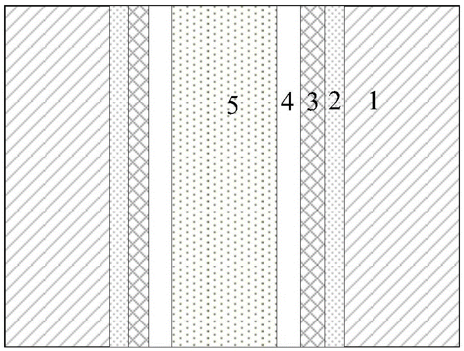
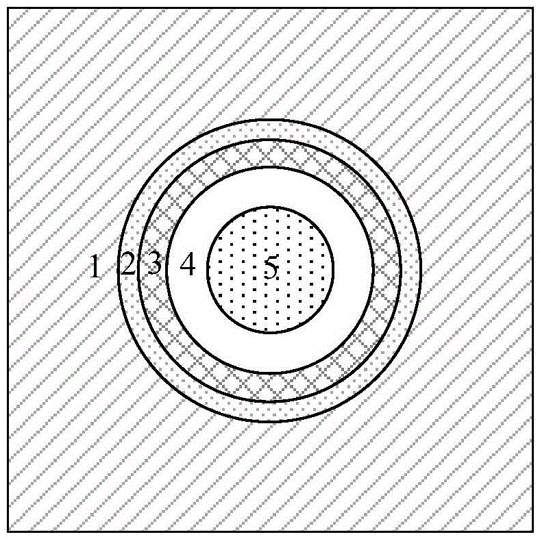
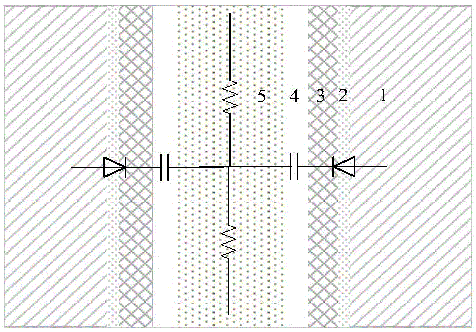
[0058] Step 1. Select a P-type doped silicon substrate as the substrate 1;

[0059] Step 2. Using a reactive ion method to etch through holes that penetrate the upper and lower surfaces of the substrate 1 on the substrate 1, with a radius of 2.6 μm;

[0060] Step 3. Prepare an N-type doped layer 3 on the inner surface of the through hole formed by etching in Step 2;

[0061] Follow the steps below:

[0062] Step 3.1, using a constant surface source diffusion method to deposit impurity atoms on the inner surface of the through hole formed by etching in step 2;

[0063] Step 3.2. Use the finite surface source diffusion method to put the substrate 1 on which the impurity atoms are deposited in step 3.1 into a horizontal diffusion furnace. The furnace temperature of the horizontal diffusion furnace is 950°C, so that the impurity atoms deposited in step 3.1 are further toward The substrate 1 is diffused to form an N-type doped layer 3, and the surface concentration and doping depth of the N...

Embodiment 2

[0068] Step 1. Select a P-type doped silicon substrate as the substrate 1;

[0069] Step 2. Using a reactive ion method to etch through holes that penetrate the upper and lower surfaces of the substrate 1 on the substrate 1, with a radius of 4 μm;

[0070] Step 3. Prepare an N-type doped layer 3 on the inner surface of the through hole formed by etching in Step 2;

[0071] Follow the steps below:

[0072] Step 3.1, using a constant surface source diffusion method to deposit impurity atoms on the inner surface of the through hole formed by etching in step 2;

[0073] Step 3.2. Use the finite surface source diffusion method to put the substrate 1 on which the impurity atoms are deposited in step 3.1 into a horizontal diffusion furnace. The furnace temperature of the horizontal diffusion furnace is 1000°C, so that the impurity atoms deposited in step 3.1 are further directed toward The substrate 1 is diffused to form an N-type doped layer 3, and the surface concentration and doping depth ...

Embodiment 3

[0078] Step 1. Select a P-type doped silicon substrate as the substrate 1;

[0079] Step 2. Using a reactive ion method to etch through holes that penetrate the upper and lower surfaces of the substrate 1 on the substrate 1, with a radius of 6 μm;

[0080] Step 3. Prepare an N-type doped layer 3 on the inner surface of the through hole formed by etching in Step 2;

[0081] Follow the steps below:

[0082] Step 3.1, using a constant surface source diffusion method to deposit impurity atoms on the inner surface of the through hole formed by etching in step 2;

[0083] Step 3.2. Use the finite surface source diffusion method to put the substrate 1 on which the impurity atoms are deposited in step 3.1 into a horizontal diffusion furnace. The furnace temperature of the horizontal diffusion furnace is 1050°C, so that the impurity atoms deposited in step 3.1 are further toward The substrate 1 is diffused to form an N-type doped layer 3, and the surface concentration and doping depth of the N-...


PUM

PropertyMeasurementUnit
Thicknessaaaaaaaaaa
Radiusaaaaaaaaaa
Thicknessaaaaaaaaaa

Abstract

The invention discloses a PN junction based through-silicon-via structure. The through-silicon-via structure comprises a P type semiconductor substrate, an N type doping layer, a dielectric layer and a metal column from outside to inside in sequence; a PN junction space charge region is formed between the P type semiconductor substrate and the N type doping layer; and the N type doping layer, the PN junction space charge region and the P type semiconductor substrate form the PN junction. The invention also discloses a manufacturing method for the PN junction based through-silicon-via structure. Compared with the conventional coaxially-structured cylindrical through-silicon-via, the through-silicon-via structure in the invention adopts the PN junction formed by the N type doping layer and the P type semiconductor substrate; the through-silicon-via structure is in a reversal biasing state when a three-dimensional integrated circuit is in operating, so that an effect of noise insulation is realized automatically, and a relatively high high-frequency signal completeness is achieved; and in addition, a grounding link is saved from the through-silicon-via structure, the use of metal is reduced as well, and the thermal mechanical reliability is improved.

Description

Technical field [0001] The invention belongs to the technical field of three-dimensional integrated circuits, and specifically relates to a through silicon via structure based on a PN junction. The invention also relates to a manufacturing method of the through silicon via structure based on a PN junction. Background technique [0002] With the development of microelectronics technology, the size of microelectronic devices continues to decrease in accordance with Moore's Law, the integration of integrated circuits has gradually increased, and the performance of electronic products has been unprecedentedly improved. However, as the size is reduced to the deep submicron or even nanometer level, Moore's Law is subject to more and more challenges, including: First, the feature size of transistors gradually reaches physical limits, and quantum effects and short-channel effects are becoming more and more. Serious; secondly, as the complexity of integrated circuits and the number of tra...

Claims


Application Information

Patent Timeline
IPC IPC(8): H01L23/48H01L21/768
CPCH01L21/76877H01L23/481
Inventor 王凤娟王刚余宁梅
Owner XIAN UNIV OF TECH
Why Eureka
Try Eureka