
A through-silicon via structure based on a pn junction and its manufacturing method

A manufacturing method and a technology of through-silicon vias, which are applied in semiconductor/solid-state device manufacturing, electrical components, and electrical solid-state devices, can solve problems such as troublesome use and grounding, reduce the use of metals, improve thermomechanical reliability, and high Effects of High Frequency Signal Integrity

Inactive Publication Date: 2018-04-27
XIAN UNIV OF TECH
View PDF3 Cites 0 Cited by
  • Summary
  • Abstract
  • Description
  • Claims
  • Application Information

AI Technical Summary

Problems solved by technology

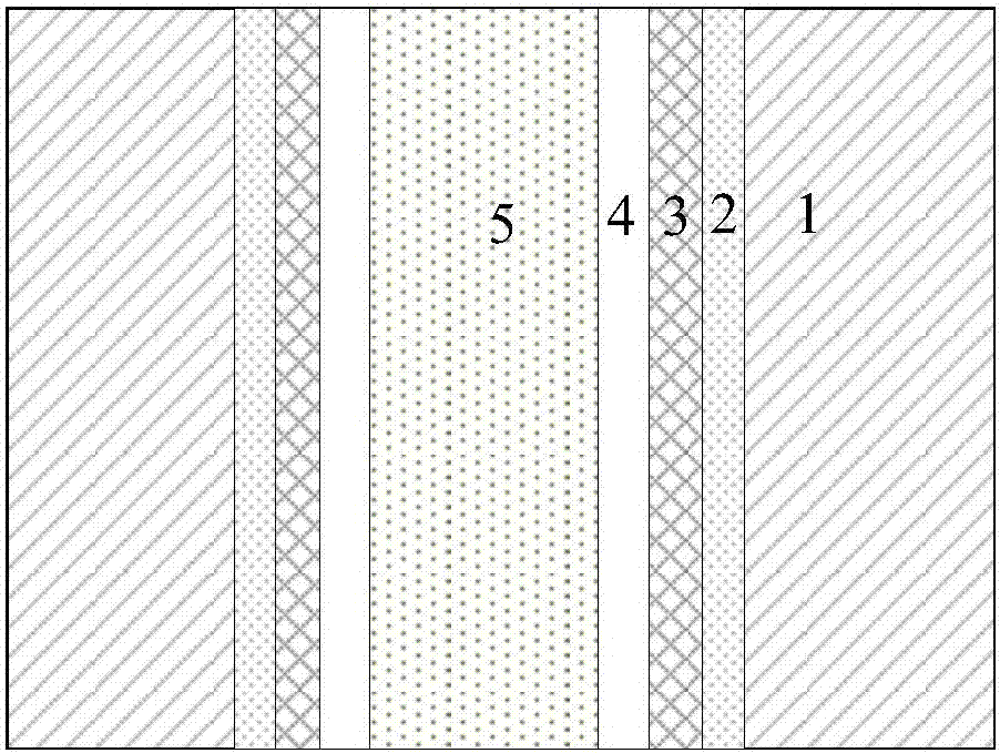
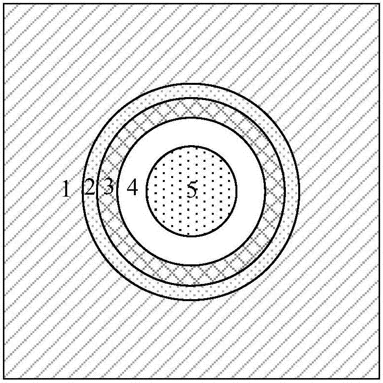
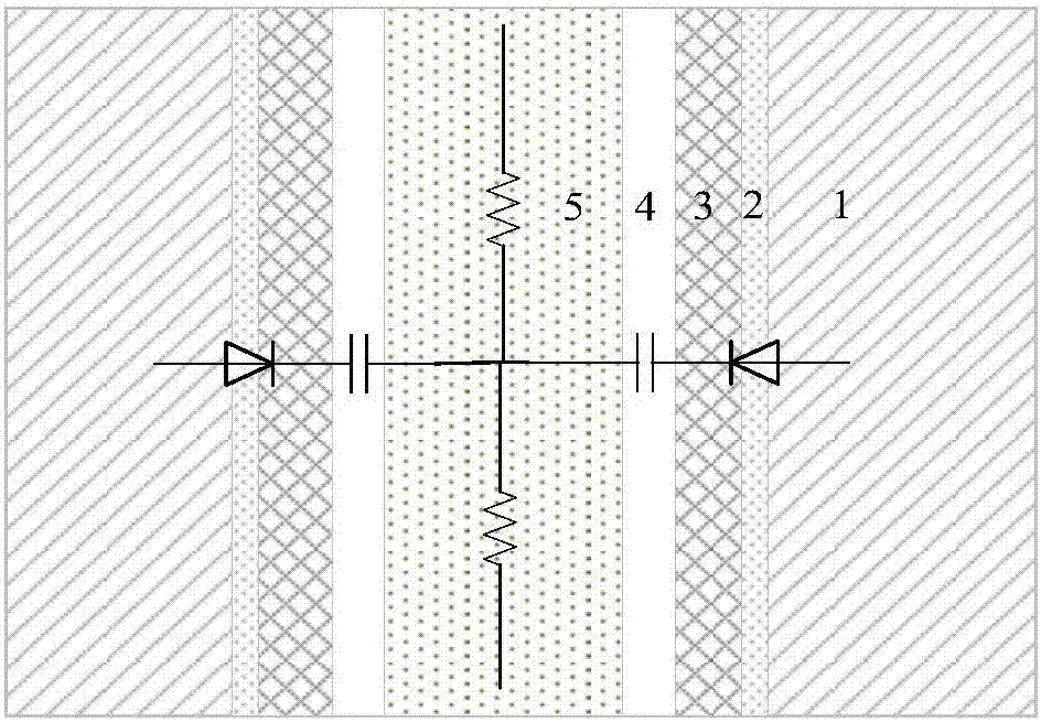
[0004] The purpose of the present invention is to provide a through-silicon via structure based on a PN junction, which solves the problem that the isolation layer of the cylindrical through-silicon via structure in the prior art must be grounded and is troublesome to use, and greatly improves the electrical reliability of the through-silicon via structure. sex

Method used


Image

  • A through-silicon via structure based on a pn junction and its manufacturing method
  • A through-silicon via structure based on a pn junction and its manufacturing method
  • A through-silicon via structure based on a pn junction and its manufacturing method

Examples


Embodiment 1

[0058] Step 1, selecting a P-type doped silicon substrate as the substrate 1;

[0059] Step 2, using reactive ion method to etch a through hole penetrating through the upper and lower surfaces of the substrate 1 on the substrate 1, the radius of the through hole is 2.6 μm;

[0060] Step 3, preparing an N-type doped layer 3 on the inner surface of the through hole formed by etching in step 2;

[0061] Specifically follow the steps below:

[0062] Step 3.1, using a constant surface source diffusion method to deposit impurity atoms on the inner surface of the through hole formed by etching in step 2;

[0063] Step 3.2: Put the substrate 1 deposited with impurity atoms in step 3.1 into a horizontal diffusion furnace by means of limited surface source diffusion. The temperature of the horizontal diffusion furnace is 950° C. The substrate 1 is diffused to form an N-type doped layer 3, and the surface concentration and doping depth of the N-type doped layer 3 are 0.5 μm.

[0064] ...

Embodiment 2

[0068] Step 1, selecting a P-type doped silicon substrate as the substrate 1;

[0069] Step 2, using reactive ion method to etch a through hole penetrating through the upper and lower surfaces of the substrate 1 on the substrate 1, the radius of the through hole is 4 μm;

[0070] Step 3, preparing an N-type doped layer 3 on the inner surface of the through hole formed by etching in step 2;

[0071] Specifically follow the steps below:

[0072] Step 3.1, using a constant surface source diffusion method to deposit impurity atoms on the inner surface of the through hole formed by etching in step 2;

[0073] Step 3.2: Put the substrate 1 on which impurity atoms have been deposited in step 3.1 into a horizontal diffusion furnace by means of limited surface source diffusion. The temperature of the horizontal diffusion furnace is 1000° C. The substrate 1 is diffused to form an N-type doped layer 3, and the surface concentration and doping depth of the N-type doped layer 3 are 1 μm....

Embodiment 3

[0078] Step 1, selecting a P-type doped silicon substrate as the substrate 1;

[0079] Step 2, using reactive ion method to etch a through hole penetrating through the upper and lower surfaces of the substrate 1 on the substrate 1, the radius of the through hole is 6 μm;

[0080] Step 3, preparing an N-type doped layer 3 on the inner surface of the through hole formed by etching in step 2;

[0081] Specifically follow the steps below:

[0082] Step 3.1, using a constant surface source diffusion method to deposit impurity atoms on the inner surface of the through hole formed by etching in step 2;

[0083] Step 3.2: Put the substrate 1 on which impurity atoms have been deposited in step 3.1 into a horizontal diffusion furnace by means of limited surface source diffusion. The temperature of the horizontal diffusion furnace is 1050° C. The substrate 1 is diffused to form an N-type doped layer 3, and the surface concentration and doping depth of the N-type doped layer 3 are 1.5 μ...


PUM


Abstract

The invention discloses a through-silicon via structure based on a PN junction, which is sequentially arranged as a P-type semiconductor substrate, an N-type doped layer, a dielectric layer and a metal column from the outside to the inside, and the connection between the P-type semiconductor substrate and the N-type doped layer The PN junction space charge region is formed between them, and the N-type doped layer, the PN junction space charge region and the P-type semiconductor substrate form the PN junction. The invention also discloses a manufacturing method of the through-silicon hole structure based on the PN junction. Compared with the cylindrical TSV of the traditional coaxial structure, the present invention adopts the N-type doped layer and the P-type semiconductor substrate to form a PN junction, which is in the reverse bias state when the three-dimensional integrated circuit is working, and automatically realizes the effect of isolating noise , to achieve higher high-frequency signal integrity. Moreover, the through-silicon via structure of the present invention omits the grounding link, reduces the use of metals, and improves thermomechanical reliability.

Description

technical field [0001] The invention belongs to the technical field of three-dimensional integrated circuits, and in particular relates to a through-silicon via structure based on a PN junction, and also relates to a manufacturing method of the through-silicon via structure based on a PN junction. Background technique [0002] With the development of microelectronics technology, the size of microelectronic devices continues to decrease according to Moore's law, the integration level of integrated circuits is gradually increasing, and the performance of electronic products has been improved unprecedentedly. However, as the size is reduced to the submicron or even nanometer level, Moore's Law is being challenged more and more, mainly including: First, the feature size of transistors gradually reaches the physical limit, and quantum effects and short channel effects are becoming more and more serious. Serious; secondly, as the complexity of integrated circuits and the number of...

Claims


Application Information

Patent Timeline
Patent Type & Authority Patents(China)
IPC IPC(8): H01L23/48H01L21/768
Inventor 王凤娟王刚余宁梅
Owner XIAN UNIV OF TECH
Learn More