
High-voltage transistor structure

A high-voltage transistor and transistor technology, applied in semiconductor devices, electric solid-state devices, semiconductor/solid-state device components, etc., can solve problems such as device failure

Inactive Publication Date: 2016-06-01
昆山矽普电子科技有限公司
View PDF9 Cites 0 Cited by
  • Summary
  • Abstract
  • Description
  • Claims
  • Application Information

AI Technical Summary

Problems solved by technology

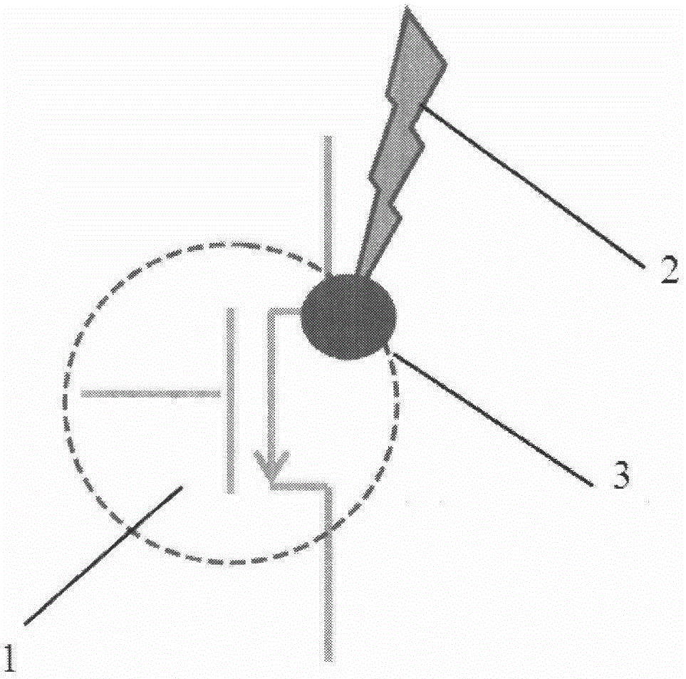
[0004] The purpose of the present invention is to provide a high-voltage transistor structure, which aims to solve the problem that the power transistor formed by the CoolMOS made of silicon material will fail due to device overvoltage or avalanche collapse caused by surge or surge.

Method used


Image

  • High-voltage transistor structure
  • High-voltage transistor structure
  • High-voltage transistor structure

Examples


Embodiment Construction

[0015] In order to further understand the content, features and effects of the present invention, the following examples are given, and detailed descriptions are given below with reference to the accompanying drawings.

[0016] see Figure 1 to Figure 5 :

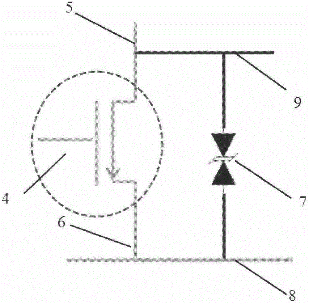
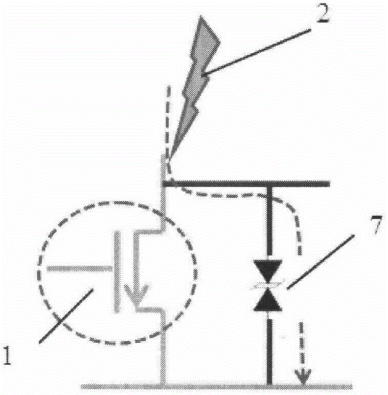
[0017] A high-voltage transistor structure includes a CoolMOS transistor 1 made of silicon material and a bidirectional high-voltage conduction protection diode 7 , and the CoolMOS transistor 1 and the bidirectional high-voltage conduction protection diode 7 are sealed in a single package 10 .

[0018] Further, the bidirectional high-voltage conduction protection diode 7 is externally connected to the source and collector of the CoolMOS transistor 1 (separately packaged), as an external protection circuit for the CoolMOS transistor 1 .

[0019] Further, the bidirectional high-voltage conduction protection diode 7 is composed of a reverse-biased high-voltage resistant diode, and the material is SiC or GaN.

[0020] Further...


PUM


Abstract

The invention discloses a high-voltage transistor structure. The high-voltage transistor structure comprises a Cool MOS transistor and a bidirectional high-voltage conduction protection diode, wherein the Cool MOS transistor is made of a silicon material; and the Cool MOS transistor and the bidirectional high-voltage conduction protection diode are packaged in a single packaging body. During the use, before the power device is damaged as extra overvoltage is generated due to surges, a bidirectional high-voltage conduction protection diode protection mechanism is started to export the extra current, so that the Cool MOS transistor is protected, and the problem that the Cool MOS transistor which is made of the silicon material loses efficacy due to the device overvoltage or snow slide collapse phenomenon caused by surges during the use can be solved.

Description

technical field [0001] The invention belongs to the field of electronic components, in particular to a high-voltage transistor structure. Background technique [0002] CoolMOS is also called SuperJunctionMOS. Because of its special structure, very low on-resistance, high voltage resistance, and low heat generation, it is also called CoolMOS. Using a new voltage-resistant layer structure, it has extremely low conduction loss while almost maintaining all the advantages of the power MOSFET. It is a structural innovation on the withstand voltage layer, which can be used not only in vertical power MOSFETs, but also in LDMOS, the key device of power IC, SBD, and other power semiconductor devices. [0003] CoolMOS is usually used in a high-voltage environment. During use, devices often fail due to device overvoltage (OverStress) or avalanche breakdown (Avalanche BreakDown) generated by surges or surges (Surge). The general solution is to extend the distance between the collector ...

Claims


Application Information

Patent Timeline
IPC IPC(8): H01L25/07H01L23/62
CPCH01L23/62H01L25/072H01L2224/49
Inventor 陈伟梵张明伦
Owner 昆山矽普电子科技有限公司
Learn More