Semiconductor device

a technology of semiconductor devices and semiconductor chips, applied in the direction of solid-state devices, transistors, basic electric elements, etc., can solve the problems of reducing the contact resistance between the power semiconductor chip and the nickel film, and reducing the service life of the power semiconductor chip. , to achieve the effect of suppressing the warp of the power semiconductor chip and simplifying the manufacturing process

Active Publication Date: 2006-05-16
ARIGNA TECH LTD
View PDF6 Cites 15 Cited by
  • Summary
  • Abstract
  • Description
  • Claims
  • Application Information

AI Technical Summary

Benefits of technology

[0017]It is an object of the present invention to ensure simplification of manufacturing process and provide a power semiconductor device capable of suppressing warp of a power semiconductor chip.
[0019]The present invention makes it possible to bond an electrode plate to each of the conductive layers with solder. Therefore, all the electrode plates can be simultaneously bonded in a manner of direct lead bonding in the same process. This allows simplification of manufacturing process. Further, since connection of all the electrode plates directly to the device with no wire such as aluminum wire becomes possible, it is possible to ensure reduction in power consumption during operation of the semiconductor device. Furthermore, since the electrode plates having high strength because of their plate-like shape are directly formed, not using aluminum wire of low strength, electrical failures such as a problematic break in the aluminum wire can be solved. Since the third conductive layer has the same layered structure as the first conductive layer has as viewed from the power semiconductor chip, the semiconductor device of the present invention can suppress warp of the semiconductor chip more effectively than conventional one by formation of the third conductive layer.

Problems solved by technology

On the second main surface side of the power semiconductor chip, formation of the nickel film directly on the second main surface causes a problem that the contact resistance between the power semiconductor chip and the nickel film should be increased.
Due to the difference of these transverse stresses, the power semiconductor chip is disadvantageously warped so that its first main surface side should become convex.
The prior-art technique on the power semiconductor device causes complication in manufacture process since a process of bonding the source electrode plate with solder and a wire-bonding process using the aluminum wire have to be performed separately.
Therefore, the prior-art power semiconductor device can not sufficiently relieve the warp of the power semiconductor chip.

Method used


Image

  • Semiconductor device
  • Semiconductor device
  • Semiconductor device

Examples


Embodiment Construction

[0025]Now, specific discussion will be made on the present invention, referring to figures showing preferred embodiments thereof.

The First Preferred Embodiment

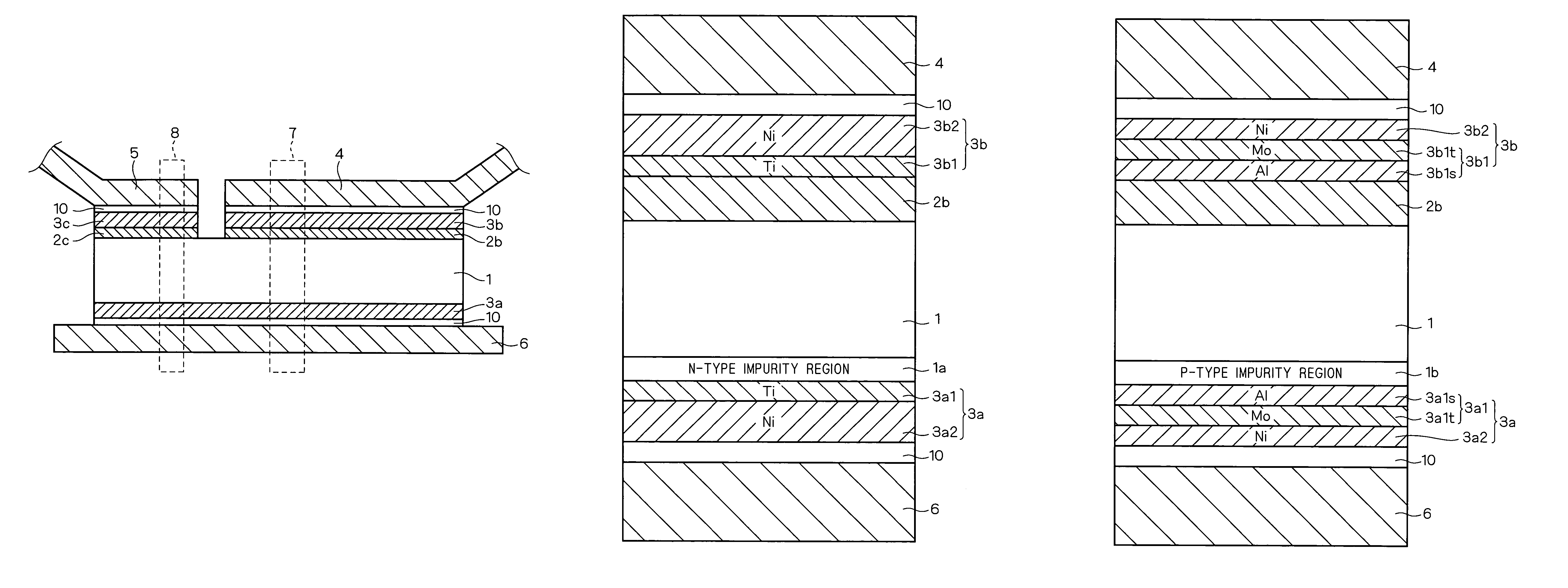
[0026]FIG. 1 is a cross section showing a structure of a power semiconductor device in accordance with the first preferred embodiment. In FIG. 1, for convenience of illustration, a package, terminals in the package, an insulating substrate below a first main electrode plate (drain electrode plate) and the like are not shown.

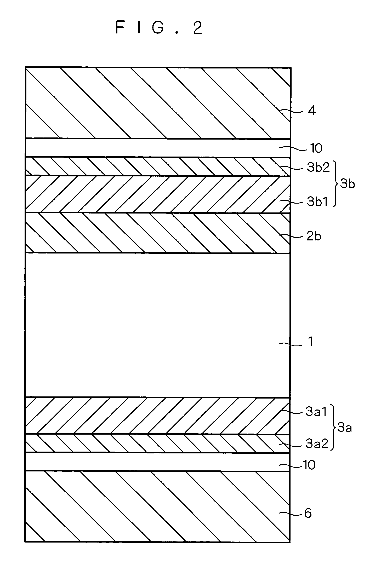
[0027]As shown in FIG. 1, on a second main surface of a power semiconductor chip 1 (on a lower surface of the power semiconductor chip 1 in FIG. 1), a first conductive layer 3a is formed. The first conductive layer 3a is bonded onto a first main electrode plate (drain electrode plate) 6 with solder 10 interposed therebetween in a manner of direct lead bonding.

[0028]The first conductive layer 3a has a layered structure consisting of a plurality of conductive films. The first main electrode plate 6 is formed ...


PUM


Abstract

A semiconductor device of the present invention comprises a semiconductor chip, metal layers formed on a first main surface of the semiconductor chip, a first conductive layer layered on a second main surface of the semiconductor chip, consisting of a plurality of conductive films, a second conductive layer layered on the metal layer, having a layered structure consisting of a plurality of conductive films formed in the same order as in the first conductive layer as viewed from the semiconductor chip and a third conductive layer layered on the metal layer, having a layered structure consisting of a plurality of conductive films formed in the same order as in the first conductive layer as viewed from the semiconductor chip. The plurality of conductive films comprise a nickel film and a low contact resistance conductive film having contact resistance with the semiconductor chip which is lower than that of the nickel film. The low contact resistance conductive film and the nickel film are formed in this order from the semiconductor chip. With such a structure, a semiconductor device ensuring simplification of its manufacturing process can be provided.

Description

BACKGROUND OF THE INVENTION[0001]1. Field of the Invention[0002]The present invention relates to a semiconductor device, and more particularly to a semiconductor device using a manner of direct lead bonding.[0003]2. Description of the Background Art[0004]In background-art power semiconductor devices, when a source electrode plate and a drain electrode plate are soldered to a power semiconductor chip, a nickel film is formed between the power semiconductor chip and each of the electrode plates in order to ensure bonding thereof using the solder.[0005]The source electrode plate is provided on the side of a first main surface of the power semiconductor chip. The drain electrode plate is provided on the side of a second main surface of the power semiconductor chip. As the power semiconductor chip, a MOSFET (Metal Oxide Semiconductor Field Effect Transistor), an IGBT (Insulated Gate Bipolar Transistor), or the like may be used.[0006]Such a method as discussed above where the source elect...

Claims


Application Information

Patent Timeline
Patent Type & Authority Patents(United States)
IPC IPC(8): H01L29/73H01L27/082H01L27/102H01L29/74H01L31/111H01L21/28H01L21/3205H01L21/60H01L23/482H01L23/485H01L23/52
CPCH01L23/4827H01L24/05H01L24/06H01L24/48H01L2924/1305H01L2924/1301H01L2924/1306H01L2924/01068H01L2224/32245H01L2224/05H01L2924/19043H01L24/29H01L24/45H01L2224/04026H01L2224/04042H01L2224/45124H01L2224/4847H01L2224/48491H01L2224/48699H01L2224/73265H01L2924/01004H01L2924/01005H01L2924/01006H01L2924/01013H01L2924/01014H01L2924/01015H01L2924/01022H01L2924/01028H01L2924/01029H01L2924/01033H01L2924/01042H01L2924/0105H01L2924/01078H01L2924/01079H01L2924/01082H01L2924/014H01L2924/13055H01L2924/13091H01L2924/14H01L2924/00014H01L2924/00H01L2224/05655H01L2224/05644H01L2224/0603H01L21/60
Inventor NARAZAKI, ATSUSHI
Owner ARIGNA TECH LTD
Why Eureka
Try Eureka