Method for reducing OLED color mixture defect and OLED display panel

A display panel and panel technology, applied in the manufacture of electrical components, electrical solid devices, semiconductor/solid devices, etc., can solve problems such as light-emitting devices not working properly, and achieve the goal of ensuring production costs, improving production yield, and reducing color mixing Effect

Inactive Publication Date: 2016-06-01
EVERDISPLAY OPTRONICS (SHANGHAI) CO LTD
View PDF6 Cites 18 Cited by
  • Summary
  • Abstract
  • Description
  • Claims
  • Application Information

AI Technical Summary

Problems solved by technology

[0010] This patent discloses a method for preparing an organic electroluminescent device, which requires the use of an evaporation process, and during the evaporation process, the evaporation material ma

Method used


Image

  • Method for reducing OLED color mixture defect and OLED display panel
  • Method for reducing OLED color mixture defect and OLED display panel
  • Method for reducing OLED color mixture defect and OLED display panel

Examples


Embodiment Construction

[0041] The specific embodiment of the present invention will be further described below in conjunction with accompanying drawing:

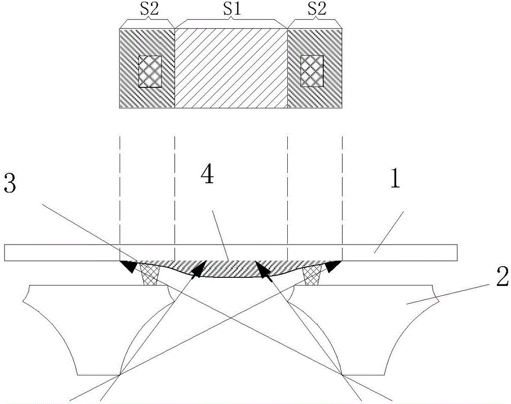
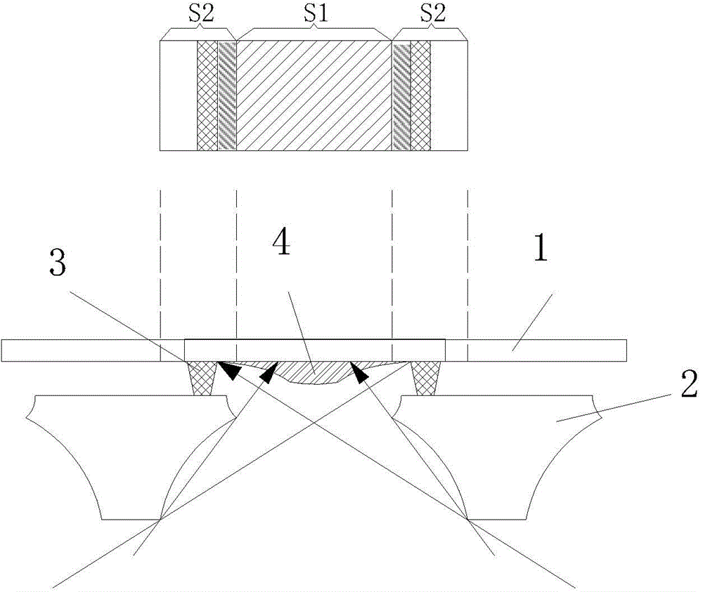
[0042] The invention provides a method for reducing OLED color mixing defects, which is applied in the OLED evaporation process, combined with figure 2 and image 3 As shown, a substrate 1 is provided, preferably, the substrate is a glass substrate.

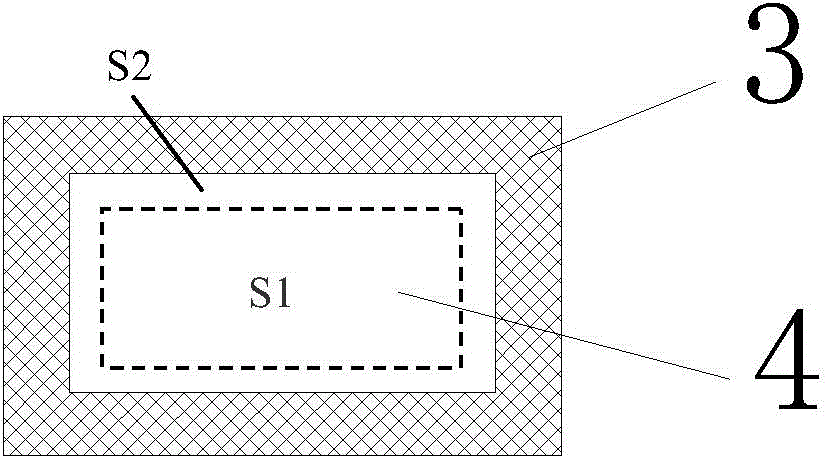
[0043] A spacer layer 3 is formed on the surface of the substrate 1, and the spacer layer 3 is adjacent to the preset evaporation area S1. Preferably, the spacer layer is a photoresist, and the spacer layer 3 is ring-shaped and the preset evaporation area S1 Surrounding, wherein, the area of ​​the preset evaporation zone S1 is smaller than or equal to the area surrounded by the spacer layer 3 .

[0044] Provide a mask plate 2 with an evaporation hole, the mask plate 2 is in contact with the spacer layer, and the evaporation hole of the mask plate 2 is aligned with the preset evaporation area S1, a...


PUM


Abstract

The present invention provides a method for reducing OLED color mixture defect and an OLED display panel. According to the method, a spacer layer is manufactured on a substrate for surrounding each evaporation area, during the process of OLED evaporation, evaporation gas only forms one layer of thin film on a preset evaporation area (i.e., a pixel unit area), and for a non-preset evaporation area (i.e., a non-pixel unit area), due to blocking of the circular spacer layer, the evaporation gas cannot enter the non-pixel unit area to cause shadow and color mixture situations, thereby improving device yield.

Description

technical field [0001] The invention relates to the field of display screen manufacturing, in particular to a method for reducing OLED color mixing defects and an OLED display panel. Background technique [0002] With the continuous development of society, mobile phones, computers, and TVs all need to use visual screens, and people's demand for display screens is also increasing. As a self-luminous display technology, OLED uses a very thin organic material coating and glass substrate. When a current passes through, these organic materials will emit light, and the OLED display screen has a large viewing angle and can significantly save power. been widely used. [0003] In the manufacturing process of OLED devices, a certain gap needs to be left between the glass substrate and the metal fine mask to avoid direct contact between the metal fine mask and the glass substrate, which will affect the light-emitting layer and cause damage to the finished product. In order to realize...

Claims


Application Information

Patent Timeline
IPC IPC(8): H01L51/56H01L27/32
Inventor 陈志豪胡友元高志豪黄俊杰
Owner EVERDISPLAY OPTRONICS (SHANGHAI) CO LTD
Why Eureka
Try Eureka