Array substrate, touch display panel and touch display device

A technology for array substrates and display areas, applied in instruments, calculations, electrical digital data processing, etc., can solve the problems of lower production efficiency, complicated manufacturing process, and increased manufacturing costs, so as to save costs, reduce process steps, and speed up manufacturing efficiency Effect

Inactive Publication Date: 2016-06-08
SHANGHAI AVIC OPTOELECTRONICS +1
View PDF9 Cites 53 Cited by
  • Summary
  • Abstract
  • Description
  • Claims
  • Application Information

AI Technical Summary

Problems solved by technology

[0004] In the prior art touch display device, since the touch wiring needs to be set separately, the entire manufacturing process becomes more

Method used


Image

  • Array substrate, touch display panel and touch display device
  • Array substrate, touch display panel and touch display device
  • Array substrate, touch display panel and touch display device

Examples


Embodiment Construction

[0032] The present invention will be further described in detail below in conjunction with the accompanying drawings and embodiments. It should be understood that the specific embodiments described here are only used to explain the present invention, but not to limit the present invention. In addition, it should be noted that, for the convenience of description, only some structures related to the present invention are shown in the drawings but not all structures.

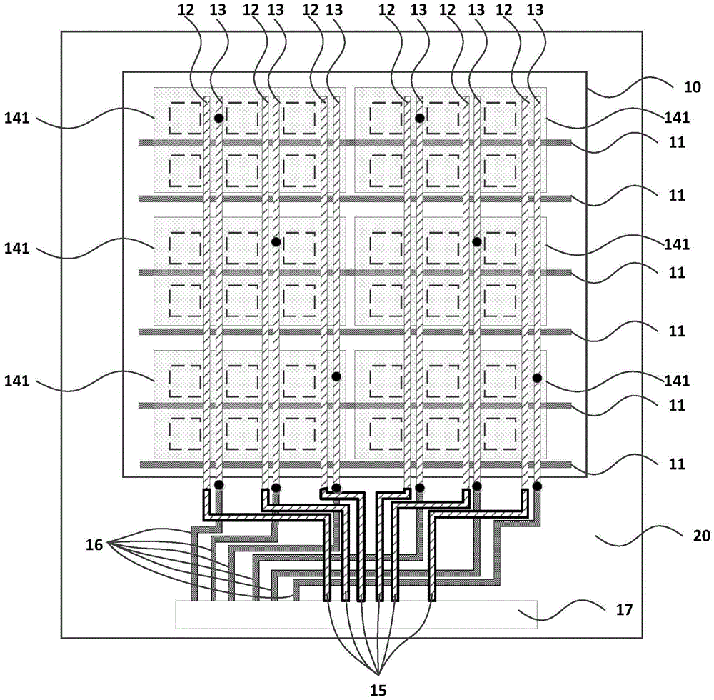
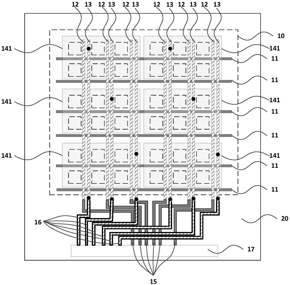
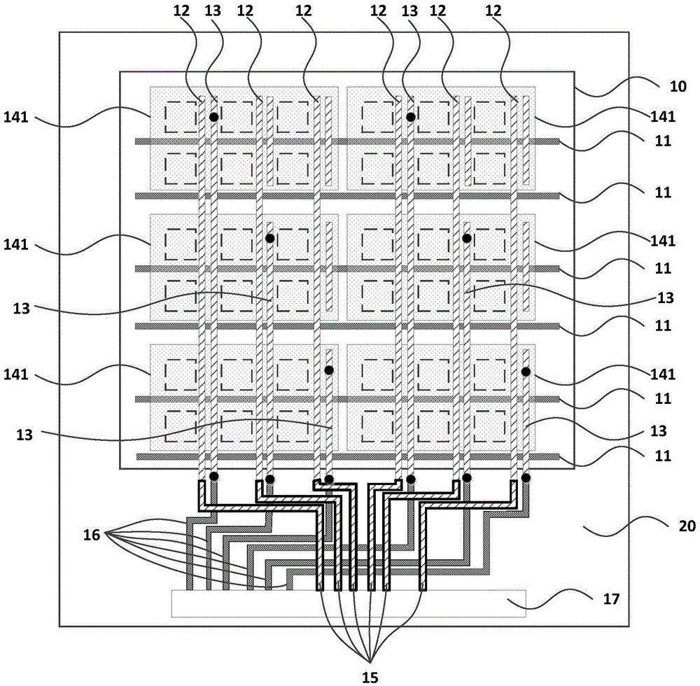
[0033] figure 1 A schematic structural diagram of an array substrate provided by an embodiment of the present invention. see figure 1 As shown, the array substrate includes a display area 10 and a peripheral circuit area 20 surrounding the display area. The display area 10 is provided with a plurality of scan lines 11 , a plurality of data lines 12 and a plurality of touch wires 13 which are insulated from each other. The array substrate further includes a touch electrode layer (not shown), and the touch electr...


PUM


Abstract

The invention discloses an array substrate, a touch display panel and a touch display device. The array substrate comprises a display region and a peripheral circuit region around the display region, and further comprises a plurality of scanning lines, a plurality of data lines and a plurality of touch leads, wherein the scanning lines, the data lines and the touch leads are located in the display region and are mutually insulated; a touch electrode layer comprises a plurality of touch electrode blocks, and each touch electrode block is correspondingly and electrically connected with at least one touch lead; the touch leads are arranged in the same layer with the data lines, and extension directions of the touch leads are parallel to extension directions of the data lines; the data lines and the touch leads are connected with corresponding interfaces of a drive chip through first adapter lines and second adapter lines respectively; the first adapter lines and the second adapter lines are located in the peripheral circuit region of the array substrate; the first adapter lines are arranged in the same layer with the data lines, and the second adapter lines are arranged in the same layer with the scanning lines; or the second adapter lines are arranged in the same layer with the data lines, and the first adapter lines are arranged in the same layer with the scanning lines. The array substrate reduces technological processes, and lowers the production cost.

Description

technical field [0001] The embodiments of the present invention relate to the technical field of touch display, and in particular, to an array substrate, a touch display panel and a touch display device. Background technique [0002] Liquid crystal display, commonly known as LCD (Liquid Crystal Display) in English, is a kind of flat-panel display. With the development of science and technology, LCD is also developing towards the goal of being light, thin, short, and small. Whether it is a wide viewing angle display, low power consumption, small size, or zero radiation, etc., users can enjoy the best Visual effects. [0003] A display with a touch function is produced based on a function-enriching technology. Common touch technologies include In-cell touch technology and On-cell touch technology. Among them, the In-cell touch technology refers to the technology of embedding the touch panel function inside the liquid crystal display panel, and the On-cell touch technology re...

Claims


Application Information

Patent Timeline
IPC IPC(8): G02F1/1333G02F1/1343G02F1/1362G06F3/041
CPCG02F1/13338G02F1/1343G02F1/136286G06F3/0412
Inventor 席克瑞崔婷婷张敏
Owner SHANGHAI AVIC OPTOELECTRONICS
Why Eureka
Try Eureka