Power good signal output method and power good signal output device

A signal output and signal technology, which is applied in the field of power supply signal output method and device, can solve the problems affecting the accuracy of power supply status judgment, affecting the overall performance of display driver chips, and protecting circuit misoperation, so as to solve the problem of competition and risk , Eliminate burr phenomenon, the effect of zero power consumption quiescent current

Active Publication Date: 2016-06-08
GALAXYCORE SHANGHAI
View PDF5 Cites 2 Cited by
  • Summary
  • Abstract
  • Description
  • Claims
  • Application Information

AI Technical Summary

Problems solved by technology

[0012] It can be seen that due to the competition and risk problems caused by the different delays of the enable switch and the judgment module, there will be glitches in the actual response output (t1-t2

Method used


Image

  • Power good signal output method and power good signal output device
  • Power good signal output method and power good signal output device
  • Power good signal output method and power good signal output device

Examples


Embodiment 1

[0078] FIG. 7(A) shows the circuit diagram of the power good signal output subunit of Embodiment 1 of the present invention, and FIG. 7(B) shows the effect diagram of the power good signal output subunit of Embodiment 1 of the present invention.

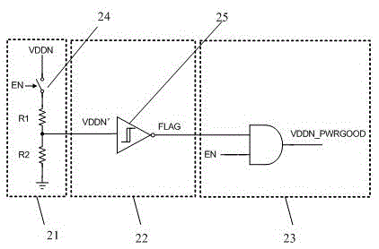
[0079] As shown in Figure 7(A), the power good signal output subunit of the present invention includes a voltage divider module 221 with an enable switch 224, a forward judgment module 222 and a trigger 223, wherein the enable switch 224 is close to the ground wire terminal (GND terminal).

[0080] Wherein, the voltage dividing module 221 converts the input power supply voltage VDDN into a detection divided voltage VDDN' that can be judged by dividing the voltage by resistors. Since the voltage divider module 221 is provided with an enable switch 224 responsive to the enable signal EN, the static power consumption of the voltage divider resistor string can be zero in deep sleep or shutdown mode through the control of the enable signa...

Embodiment 2

[0089] FIG. 8(A) shows the circuit diagram of the power good signal output subunit of the second embodiment of the present invention, and FIG. 8(B) shows the effect diagram of the power good signal output subunit of the second embodiment of the present invention.

[0090] As shown in FIG. 8(A), the power good signal output subunit of the present invention includes a voltage divider module 321 with an enable switch 324, a forward judgment module 322 and a trigger 323, wherein the enable switch 324 is close to the power supply voltage end (VDDN end).

[0091] Wherein, the voltage dividing module 321 converts the input power supply voltage VDDN into a detection divided voltage VDDN' that can be judged by dividing the voltage by resistors. Since the voltage divider module 321 is provided with an enable switch 324 that responds to the enable signal EN, the static power consumption of the voltage divider resistor string can be zero in deep sleep or shutdown mode through the control ...

Embodiment 3

[0100] FIG. 9(A) shows the circuit diagram of the power good signal output subunit of the third embodiment of the present invention, and FIG. 9(B) shows the effect diagram of the power good signal output subunit of the third embodiment of the present invention.

[0101] As shown in Figure 9(A), the power good signal output subunit of the present invention includes a voltage divider module 421 with an enable switch 424, a reverse judgment module 422 and a trigger 423, wherein the enable switch 424 is close to the power supply voltage end (VDDN end).

[0102] Wherein, the voltage dividing module 421 converts the input power supply voltage VDDN into a detection divided voltage VDDN' that can be judged by dividing the voltage by resistors. Since the enable switch 424 is provided in the voltage divider module 421 in response to the enable signal EN, the static power consumption of the voltage divider resistor string can be zero in deep sleep or shutdown mode through the control of ...


PUM


Abstract

The invention provides a power good signal output method and a power good signal output device. The power good signal output device comprises the components of a voltage bleeding module which is provided with an enabling switch and is used for converting an input power voltage to a detecting sub-voltage for determination, wherein the enabling switch responds to the enabling signal, and the power voltage is positive or negative; a forward determination module or a backward determination module which is used for determining the detecting sub-voltage and outputting a mark signal; and a trigger which is used for processing the enabling signal and the mark signal and outputting the power good signal. According to the power good signal output method and the power good signal output device, the enabling signal and the mark signal are processed by means of the trigger for outputting the power good signal. Not only can zero-power-consumption static current realized in a deep-sleep or shutdown manner, but also a competition problem and a risk problem caused by different time delays of the enabling switch and a determining module can be settled. The power good signal output method and the power good signal output device have advantages of eliminating a burr phenomenon in actual response output, improving determination accuracy for the power good state, and improving integral performance of a display driving chip.

Description

technical field [0001] The invention relates to the field of integrated circuits, in particular to a power good signal output method and device. Background technique [0002] With the increasing popularity of smart phones, people have higher and higher requirements for the display effect of mobile smart terminals, and the display effect of wide screen and high resolution with high performance has become the mainstream. Therefore, more and more challenges are raised to the functions and performance of the display driver chip of the handheld device. [0003] The charge pump in the multi-output power management unit, which is very important in the display driver chip, provides positive and negative bias voltages for the liquid crystal. During the process of power-on or power-off, the charge pump module needs to be charged and discharged for several clock cycles to achieve Therefore, it is particularly important to detect the states of the multiple positive and negative output ...

Claims


Application Information

Patent Timeline
IPC IPC(8): G09G3/20
CPCG09G3/2077
Inventor 张科王富中丁启源
Owner GALAXYCORE SHANGHAI
Why Eureka
Try Eureka