Supercharge Your Innovation With Domain-Expert AI Agents!

Lead wire framework used for packaging structure without pin and manufacturing method thereof, and packaging structure

A leadless packaging and lead frame technology, used in semiconductor/solid-state device manufacturing, electrical components, electrical solid-state devices, etc., can solve the problems of frame yield loss, poor plating, frame deformation, etc., and improve the wiring layout. , shorten the length of the line, the effect of reasonable structure design

Inactive Publication Date: 2016-06-08
SHANGHAI KAIHONG ELECTRONICS CO LTD +2
View PDF5 Cites 1 Cited by
  • Summary
  • Abstract
  • Description
  • Claims
  • Application Information

AI Technical Summary

Problems solved by technology

However, the thickness of the current pre-packaged frame cannot be less than 0.127mm due to the limitation of the packaging capacity; the increase of the pre-packaged process will further cause the yield loss of the finished frame (over glue, frame deformation, poor coating, etc.); based on different frame thicknesses and frame shapes Dimensions require investment in different prepackaged molds

Method used


Image

  • Lead wire framework used for packaging structure without pin and manufacturing method thereof, and packaging structure
  • Lead wire framework used for packaging structure without pin and manufacturing method thereof, and packaging structure
  • Lead wire framework used for packaging structure without pin and manufacturing method thereof, and packaging structure

Examples


Embodiment Construction

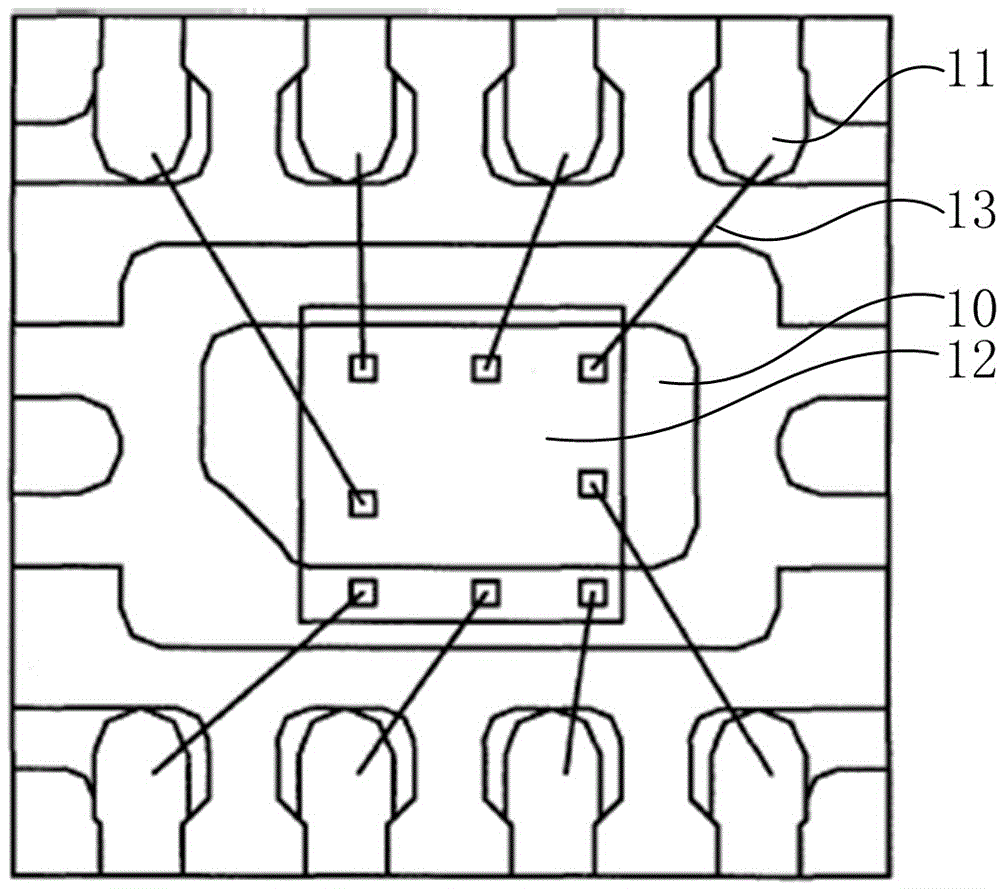
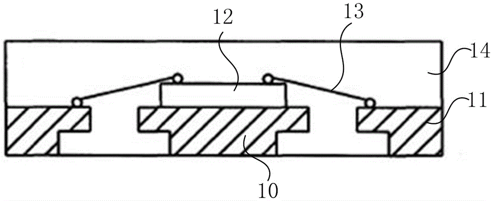
[0022] The specific implementations of the lead frame for the leadless packaging structure, the manufacturing method and the packaging structure provided by the present invention will be described in detail below in conjunction with the accompanying drawings. The accompanying drawings are only used to illustrate the structure of the lead frame of the present invention, and are not used to limit the dimensional relationship among the various components of the present invention.

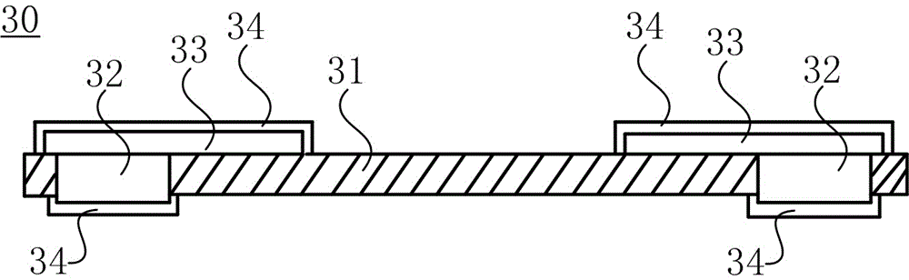
[0023] see image 3 , the lead frame 30 used in the leadless packaging structure of the present invention includes a frame body 31 and a plurality of conductive posts 32 penetrating through the frame body 31 .

[0024] The lead frame body 31 is made of an insulating material, and the insulating material may be an insulating material known in the prior art, which is not limited in the present invention. In this specific embodiment, the frame body 31 is relatively thin and is a film frame body.

[0025...


PUM


Abstract

The invention provides a lead wire framework used for a packaging structure without a pin and a manufacturing method thereof, and the packaging structure. The lead wire framework comprises a framework body and a plurality of conductive piles penetrating the framework body. One surface of the framework body is provided with a conductive bonding pad electrically connected to the conductive piles. A position on the surface of the framework body, which is not provided with the conductive bonding pad, is used for placing a chip. The conductive bonding pad is electrically connected to the chip through a metal line. The framework body is made of an insulating material. The framework, the method and the structure have advantages that the insulation lead wire framework body is used to support the chip; after plastic packaging, there is no exposed base island; a QFN / DFN packaging demand without the exposed base island can be realized; a structure design of the framework is reasonable; wiring layout is effectively improved, a wire length is shortened and a wiring risk is reduced; a space in a plastic packaging body can be effectively used so as to realize packaging of a small size packaging body; there is no metal on a cutting channel, an arrangement density is high and cost is effectively reduced.

Description

technical field [0001] The invention relates to the field of semiconductor packaging, in particular to a lead frame for a leadless packaging structure, a manufacturing method and a packaging structure. Background technique [0002] In the prior art, QFN (QuadFlatNolead) is a square flat no-lead semiconductor chip packaging structure, and its internal top view structure is as follows: figure 1 As shown, the cross-sectional structure is as follows figure 2 shown. It can be seen from these two views that the packaging structure is composed of a central base island 10 and conductive pads 11 arranged around the base island 10 in the lower part of the chip packaging space. The chip 12 is placed on the base island 10, and the Each conductive portion is electrically connected to each conductive pad 11 through a metal wire 13 , and epoxy resin 14 is filled in the rest of the packaging space. DFN (DualFlatNolead) is a rectangular flat no-lead semiconductor chip packaging structure...

Claims


Application Information

Patent Timeline
Patent Type & Authority Applications(China)
IPC IPC(8): H01L23/495H01L23/488H01L21/60
CPCH01L2224/48091H01L2224/48247H01L2224/73265H01L2924/181
Inventor 吴畏阳小芮
Owner SHANGHAI KAIHONG ELECTRONICS CO LTD
Features
  • R&D
  • Intellectual Property
  • Life Sciences
  • Materials
  • Tech Scout
  • Unparalleled Data Quality
  • Higher Quality Content
  • 60% Fewer Hallucinations
Learn More